

When you send a design to a PCB fabricator under a build-to-print agreement, the files become the contract. The manufacturer follows them exactly, and responsibility for anything they leave out stays with you.
This guide explains how the build-to-print PCB manufacturing process works for bare boards. You will find the files a fabricator needs and the tolerances most shops hold. A quote checklist at the end keeps every supplier pricing the same board.
What Is Build-to-Print PCB Manufacturing?
Build-to-print PCB manufacturing is a production model where the customer completes the design, and the manufacturer builds the printed circuit board exactly as documented. The customer retains design authority and controls revisions, and the manufacturer is responsible for meeting the agreed manufacturing tolerances and quality requirements.

This differs from build-to-spec manufacturing, where the customer defines performance requirements, and the supplier takes responsibility for developing a suitable design. Intellectual property ownership and liability depend on the contractual agreement.
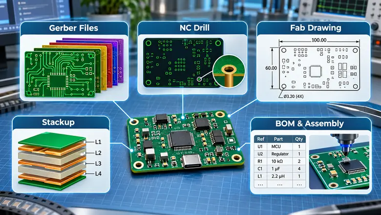
For example, an industrial controller manufacturer may submit Gerber files, drill data, a stackup, and fabrication drawings specifying the required IPC class. The fabricator reviews these documents for manufacturability and raises any concerns before production. If the drill data conflicts with the drawing, the customer must resolve the discrepancy and approve the necessary changes.
Build-to-print manufacturing can cover bare PCB fabrication or extend to assembly as well. Assembly projects also require a bill of materials (BOM) and assembly drawing with component placement files.
What Files Are Required for Build-to-Print PCB Manufacturing?
A complete manufacturing package gives the manufacturer enough information to reproduce the approved design. Each file serves a different purpose, so missing information in one document can affect the entire production process.
1. Gerber Files
Gerber files define the patterns needed to manufacture a PCB, including copper traces and solder mask openings. They also contain silkscreen markings used for component identification. Also, each PCB layer usually has a separate Gerber file, with the board outline included in the fabrication package.
Before sending the files to a PCB manufacturer, designers should review them in a Gerber viewer. This helps identify missing layers or alignment issues. The board outline should also be checked to ensure it matches the intended design.
Some manufacturers also support formats such as ODB++ or IPC-2581, which can include additional design information. However, designers should confirm that their chosen supplier accepts these formats before submission.
2. NC Drill Files
NC drill files in the build-to-print PCB manufacturing package specify the hole locations and diameters needed for PCB manufacturing. These holes accommodate component leads and mounting hardware, while smaller drilled holes are often used to form vias.
The files should distinguish plated-through holes from non-plated holes. Any slots or special drilling requirements must also be specified to prevent manufacturing errors.
Designers should confirm whether the stated hole diameter refers to the finished size after plating. Incorrect dimensions can make it difficult to insert component leads or install mounting hardware.
3. PCB Fabrication Drawing
A PCB fabrication drawing provides manufacturing instructions that Gerber files alone cannot fully describe. It defines the finished board dimensions and thickness, along with the required materials and surface finish.
The drawing should also specify the layer arrangement and dielectric requirements for multilayer PCBs. Any special PCB manufacturing processes or inspection requirements should be included in the fabrication notes.
Each drawing must have a document number and revision identifier. This helps manufacturers confirm they are working with the latest approved design and prevents confusion during production.
4. Layer Stackup and Material Specifications
The PCB stackup defines how copper layers are arranged within the board and separated by insulating materials. This arrangement affects the board’s electrical performance and overall thickness. It also influences manufacturing complexity.
Designers should specify the copper weight for each layer and the required laminate properties. When there are designs with controlled impedance, the documentation must identify the target impedance and relevant signal layers.
For example, a six-layer PCB may require specific dielectric thicknesses to achieve the intended impedance. These requirements should be communicated to the manufacturer before fabrication.
If alternative materials are acceptable, they should be clearly identified. Otherwise, the manufacturer must obtain approval before making substitutions.
5. Bill of Materials and Assembly Files
PCB assembly requires additional documentation to ensure components are well-sourced and placed on the board.
The bill of materials (BOM) identifies the components needed for assembly, including their manufacturer part numbers and quantities. Each part must be linked to its reference designator on the PCB. Approved alternatives should also be listed, while components that must remain unpopulated should be marked as do-not-populate (DNP).
For automated assembly, pick-and-place files provide the component coordinates and rotation angles. They also indicate which side of the PCB each component belongs to.
An assembly drawing complements these files by showing component orientation and any special installation instructions that automated placement data may not fully describe.
Which PCB Manufacturing Tolerances Should Be Specified?
PCB manufacturing processes introduce small dimensional variations. These become important when a PCB must fit an enclosure or connect to precision mechanical components.
In build-to-print PCB manufacturing, the customer should specify critical tolerances in the fabrication documentation. The manufacturer can then confirm whether its equipment and processes can meet them.
The following table summarizes common requirements.
| CB Feature | Tolerance or Requirement to Define | Typical Tolerance Values |
| Board dimensions | Finished length, width, and outline tolerance | ±0.10–0.20 mm for CNC routing |
| Board thickness | Nominal finished thickness and permitted variation | ±10% for boards ≥1.0 mm thick |
| Hole dimensions | Finished hole diameter, tolerance, and plating status | ±0.075–0.10 mm for many plated holes |
| Copper traces | Minimum trace width and spacing | 0.10/0.10 mm minimum width/spacing is common; trace width tolerance around ±20% |
| Copper thickness | Required finished copper thickness per layer | 1 oz ≈35 µm nominal; finished thickness acceptance depends on specification |
| Layer registration | Allowable alignment variation between layers | Approximately ±0.05–0.13 mm |
| Controlled impedance | Target impedance and acceptable tolerance | ±10% typical; ±5% available with tighter process control |
| Slots and cutouts | Finished dimensions and positional tolerances | Approximately ±0.10–0.20 mm for routed features |
Note: These figures are general industry reference values for conventional rigid PCBs, not guaranteed tolerances for every manufacturer. These values should come from the design requirements and be reviewed against the fabricator’s capabilities.
How Do Tolerances Affect PCB Manufacturing Cost?
Tighter tolerances can increase manufacturing costs because they demand closer process control and additional inspection.
Small drilled holes or narrow trace spacing may require specialized equipment. Higher layer counts and controlled-impedance requirements can also increase production complexity.
The goal is to specify the precision the product actually needs. Applying unusually strict tolerances to every dimension can increase the quote without improving the board’s functional performance.
Build-to-Print PCB Manufacturing Quote Checklist
An accurate PCB quote starts with a complete request for quotation (RFQ). Every supplier should receive the same design files and manufacturing specifications so buyers can compare prices under consistent conditions.
Use the following checklist when preparing your RFQ for build-to-print PCB manufacturing:
| RFQ Item | Information to Include |
| Manufacturing files | Gerber, ODB++, or IPC-2581 data, NC drill files, board outline, and IPC-D-356 netlist if available |
| Design documentation | Approved fabrication drawing, stackup, part number, and revision |
| Board specifications | Layer count, laminate material, Tg, copper weight, finished thickness, and surface finish |
| Tolerances | Critical dimensional tolerances, hole requirements, and applicable IPC class |
| Controlled impedance | Target impedance, acceptable tolerance, and any test report requirements |
| Special processes | Via filling, gold fingers, countersinks, edge plating, or other special features |
| Quantity and panelization | Order quantity, expected production volumes, and panel or array preferences |
| Testing and inspection | Electrical testing, required inspection methods, and quality documentation |
| Assembly requirements (if applicable) | BOM, placement files, assembly drawings, and component sourcing responsibilities |
| Delivery requirements | Required lead time, shipping destination, packaging, and labeling instructions |
Even small specification differences can affect custom PCB cost. For example, changing the copper weight or laminate material may increase manufacturing costs and production time.
When comparing quotations, check what each supplier includes in the final price. A lower quote may exclude electrical testing or freight charges. Similarly, material substitutions can affect the board’s specifications. Also, ask suppliers to identify any deviations from the approved design and provide a lead-time breakdown covering the manufacturing stages included in the order.
What Happens After You Submit the Manufacturing Files?
When the manufacturer receives the files, a CAM (Computer-Aided Manufacturing) engineer reviews them for accuracy and manufacturability. This involves checking board dimensions, drill data, trace spacing, and annular rings against the specified requirements and manufacturing capabilities.
The engineer also verifies whether the proposed stackup for multilayer boards can meet the required thickness and impedance targets during the PCB fabrication process.
If the review identifies a problem, the manufacturer issues an engineering query (EQ) requesting clarification. For example, a copper trace may be too close to the board edge, or the specified stackup may need adjustment to achieve the target impedance.

The customer must approve any changes affecting the released design before production. These approvals should be documented through the appropriate revision or deviation records. Some high-reliability projects also follow a copy exact approach, which prohibits unauthorized changes to materials or manufacturing processes.
Before production begins, the customer and manufacturer should also agree on inspection and acceptance requirements. For rigid PCBs, IPC-6012F defines performance requirements, while IPC-A-600K provides visual acceptance criteria. Electrical testing helps identify open circuits and short circuits, with additional inspection reports required for certain designs.
Common Mistakes That Delay Build-to-Print PCB Orders
Manufacturing delays frequently begin with documentation problems that could have been resolved before the RFQ.
One common issue is submitting files from different design revisions. The Gerber data may represent the latest layout, but the fabrication drawing still describes an earlier board thickness or hole arrangement.
Another problem occurs when critical requirements are missing. A supplier may need to clarify the surface finish or request additional information about controlled impedance before preparing a reliable quote.
Assembly orders face similar difficulties when component part numbers are incomplete, or placement data does not match the BOM.
A final review of the complete manufacturing package helps catch these inconsistencies before submission.
Conclusion
Build-to-print PCB manufacturing depends on clear documentation and well-defined production requirements. Complete fabrication files allow manufacturers to understand the design. Plus, the agreed tolerances and inspection criteria establish what the finished board must meet.
We at LHD TECH support customer-defined PCB manufacturing projects through PCB fabrication, component sourcing, and precision SMT and through-hole assembly. Contact us with your Gerber or ODB++ files, drill data, netlist, drawing and stackup, and the engineering team will review the package and offer a customized PCB manufacturing quote.