Introduction to Dual Inline Package (DIP)
Dual Inline Package, is a fundamental packaging technology in the electronics industry. When observing PCBs, especially in old computers, microcontroller development boards, or educational electronic devices, one often sees rectangular black chips with parallel pins on both sides. These PCBs and components using dual inline packages are classic designs changed the field of electrical engineering.
What is The Dual Inline Package Meaning?
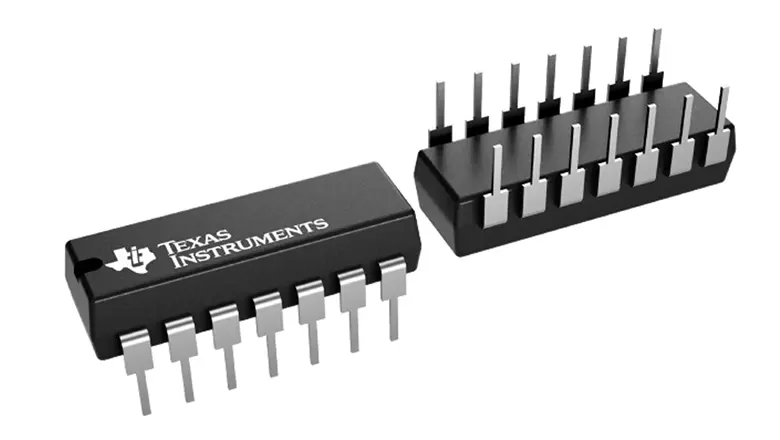
In various electronic packaging forms, DIP occupies a unique position due to its practicality, ease of use, and important historical. It provides a stable, reliable, and scalable packaging solution for many electronic products, widely used from early personal computers to today’s prototype development boards. Although surface mount technology (SMT) and fine-pitch surface mount components (SMD) are becoming prevalent, this type of packaging remains indispensable in prototyping, educational experiments, repair and replacement, and industrial control.
This article will include the definition, pruduction process, internal structure, pin count, internal components, technological development, characteristics, application scenarios, also ompare DIP with SOIC and other packaging forms. After reading this article, you will not only understand the working principle of DIP packaging, but also be able to use DIP components more proficiently in actual electronic projects and perform effective troubleshooting.
What is a Dual Inline Package?

Dual inline package(DIP) refers to a type of integrated circuit package characterized by two rows of parallel metal metal leads extending from both sides of a rectangular package. This lead layout gives the name “dual in-line package,” with “in-line” being a direct description of the two rows of parallel leads.
Function of the DIP
- Electrical Connections: Each pin works as a connection point for the IC or component inside the package to the The pins are pluged into holes on a PCB (printed circuit board), soldered for a safe connection.
- Mechanical Stability: The two parallel rows will support the package on circuit board, holding it steady and reducing physical stress on the PCB and the chip
- Socket Compatibility: DIPs can be inserted into sockets (can easy replacement/repair) or soldered directy to the board.
Why Choose a DIP Package?
A DIP package is a common choice for electronic devices because:
- It supports rapid prototyping.
- It’s easy to repair by swapping chips.
- It works with most educational and breadboard setups due to its standardized pin pitch.
DIP Package at a Glance
| Feature | Description |
| Configuration | Two parallel rows of pins |
| Pin Pitch | 2.54 mm (0.1 inch) standard |
| Pin Count | Even numbers (typically 8 to 64) |
| Use | Integrated circuits, logic devices, etc. |
| Mounting | Through-hole on PCB or socket |
| Sockets | Supported for easy replacement |
The History of DIP Packaging
Invention of the DIP
The history of dip packaging begins in 1964 with Texas Instruments. Their engineers—Rex Rice, Don Forbes, and Bryant Rogers—developed the original DIP to streamline IC mounting on PCBs. This breakthrough earned “dual in-line package” status in electronics history and became the default component package for decades.
Milestones in the Evolution of DIP
- 1960s–1970s: Early DIPs replaced awkward round TO-5 cans and “flat packs,” establishing a uniform system for PCB assembly.
- 1980s: The spread of home computing and microprocessors. DIP chips seems like the Intel 8080 or Zilog Z80 set design standards.
- 1990s: DIP continued to be usually available in prototyps, educational kits, and repair/maintenance spares SMT packages began dominating new desig.
- 2000s–Today: While mass-market consumer devices switched to SMDs, DIP technology is still heavily relied on in retro-computing, DIY hardware, repair-centric industries, and classrooms.
Advantages of DIP’s Historical Design
- Made circuit board manufacturing easier and more reliable.
- Allowed mass adoption of digital electronics, due to the ease of handling and assembly.
- Facilitated component replacement and repair (inserted into a socket).
Structure of DIP Package: Inside the Package

Let’s “open up” the package and see what’s inside a DIP.
Essential Structure Elements
- Package Body: Made from plastic epoxy (PDIP, plastic dual in-line package) or ceramic (CDIP, ceramic dual), enclosing the precious integrated circuit.
- Silicon Die: The heart of the DIP package is the silicon die, where the actual integrated circuit or electronic function lives.
- Wire Bonds: Ultra-fine wires (often gold or aluminum) connect the silicon die’s terminals to the lead frame.
- Lead Frame: Metal arms embedded in the package body, carrying signals to the package supports—the external pins.
- Pins in a DIP: The notable “legs,” arranged in two parallel rows at the sides of the package.
- Package Substrate: This often refers to internal supporting layers for rigidity, sometimes with multi-layer ceramic types for extreme environments.
DIP vs. SOIC and SOP Package Structure
| Feature | DIP | SOIC (Small Outline) / SOP Package |
| Mounting | Through-hole, socket | Surface-mount (SMD/SMT) |
| Pin Count Range | 8–64 (even number) | 8–56, higher density |
| Compatibility | Breadboard, sockets | Not breadboard friendly |
| Repairability | Excellent | Requires specialized equipment |
| Physical Size | Larger | Smaller, thinner profile |
| Package Components | Pins, die, package body | Pins/”gull wing” leads |
Types and Variations: Plastic DIP, Ceramic DIP, Shrink DIP, and More

Dual inline packages are designed to fit a wide array of applications, environments, and even legacy standards. DIP packaging components are also made to accommodate special requirements regarding durability, temperature tolerance, and space constraints.
Major DIP Package Types
- Plastic Dual In-Line Package (PDIP): This is the most common DIP type—what most people picture when hearing “DIP chip.” The package body is a plastic epoxy that provides good environmental protection and mechanical strength at low cost. PDIP is favored for consumer electronics, prototyping, and many microcontrollers.
- Ceramic Dual In-Line Package (CDIP): Ceramic DIPs are chosen for environments needing excellent thermal stability and hermetic sealing, such as aerospace, industrial, or memory chips (including windowed EPROMs). Ceramic dual packages offer superior moisture and chemical resistance as well.
- Shrink DIP / Skinny Dual In-Line Packages: Shrink DIPs, also called Skinny DIPs, feature a narrower body and smaller pin pitch to save board space—making them popular for denser PCB layouts without sacrificing the benefits of DIP pin arrangement.
- Windowed Ceramic DIP: A typeof CDIP, it is a quartz window above the silicon die, It lets to UV light so EPROM memory can be erased and reprogrammed. This made early firmware and BIOS development faster, more and more flexible.
- Single-layer Ceramic DIP and Multi-layer Ceramic DIP: These are used in military and aerospaceapplications, they providde extra mechanical support, vibration resistance, and moisture-imperviousness—even when exposed to extreme temperatures conditions.
- Heat Sink DIP: This DIP variantcomes with a heat sink into or onto the package body, ideal for high-power ICs and analog chips requiring greater power dissipation.
Table: Most Common DIP Package Types
| DIP Type | Material | Typical Usage | Unique Feature |
| PDIP | Plastic | Microcontrollers, logic | Affordable, widely available |
| CDIP | Ceramic | EPROM, NASA, military | Extreme durability and reliability |
| Shrink DIP/Skinny Dual | Plastic | Compact logic, dense PCB | Space savings |
| Windowed Ceramic DIP | Ceramic | EPROM | UV-erasable data storage |
| Heat Sink DIP | Plastic/Met | Power ICs | Improved heat dissipation |
Features of Dual Inline Package: Key Properties
What features of a DIP package make it stand out as a component package?
- Package Body & Structure: Sturdy, rectangular enclosure protecting the silicon die; includes package substrate and wire bonds for maximum reliability.
- Two Parallel Rows: It is identified with its layout of leads on both sides of the package body, ensuring repeatable placement on a PCB.
- Standardized Pin Pitch: 54 mm (0.1 in.) between adjacent pins along the row, supporting the manufacturer compatibilit and easy installation.
- Even Number of Pins: DIP packages usually will have an even number of pins (8, 14, 16, 18, 24, 28, 40, 64, etc.), typically ranging from 8 up to 64.
- Socket Compatibility: A DIP can be inserted in a socket, not soldered directly, greatly reducing maintenance and repair fees.
- Physical Markers: Notch, dot, or bevel at one end for quick identification of pin 1—critical for correct circuit assembly.
- Package Uses: Microcontrollers, analog chips, microprocessors, memory, interfaces, and more.
Table: Features of a DIP Package
| Feature | Advantage |
| Two parallel rows | Symmetrical, robust PCB mounting |
| Even number of pins | Simplifies routing and layout |
| Standard pin spacing | Universal in breadboards & sockets |
| Package substrate | Supports internal chip and leads mechanically |
| Sockets supported | Enables fast replacement or upgrades |
| Well-documented standards | Supports legacy system support & repair |
Number of Pins, Pin Spacing, and Pin Numbering

The number of pins a DIP has is central to its purpose and compatibility with a given design.
Pin Count & Layout
- Ranging from 8 to 64, but DIP8, DIP14, DIP16, DIP28, and DIP40 are very common in consumer and the electronics.
- Pins will belabeled in a counter-clockwise direction from the notch or dot (Pin 1), which can ensure all packaged components be installed correctly without any mistake(vital for integrated circuit package reliability).
Pin Spacing
- Pin pitch: Standard 2.54 mm (0.1 inch) between pins in the same row, and 7.62 mm (0.3 inch) or 15.24 mm (0.6 inch) between the rows, depending on total pin count and package type.
Table: DIP Pin Arrangements
| Package Type | Number of Pins | Row Pitch | Pin Pitch |
| DIP8 | 8 | 7.62 mm | 2.54 mm |
| DIP14 | 14 | 7.62 mm | 2.54 mm |
| DIP24 | 24 | 15.24 mm | 2.54 mm |
| DIP40 | 40 | 15.24 mm | 2.54 mm |
| Shrink DIP | 8–28+ | Varies | <2.54 mm |
Dual Inline Package Installation: How to Install DIP Packages
DIP packages are easy to install whether you are a hobbyist, student, or professional.
Installing DIP (Through-Hole Mounting Steps)
- PCB Preparation: We need to ensure all holes on the printed circuit board are clear, without debris or solder.
- Align the Package: Orient the notch/dot to the board symbol, matching pin 1. Insert the IC into corresponding holes—avoid force that might bend the pins.
- Insert DIP: The package supports itself on the PCB while you flip the board to solder.
- Soldering: Solder each pin, applying heat to both pin and pad to ensure a shiny, reliable connection. Dip packages offer this assembly advantage due to large, accessible leads.
- Cleaning: Clean the flux and check for solder bridges or cold solder joints.
Socketing Options
- Insert into a socket: For experimental or frequently-swapped chips, DIPs can be inserted into ZIF (Zero Insertion Force) or standard sockets.
- Repair/Upgrade: Easily remove a failed DIP and replace it with a new one for legacy equipment repair.
Dual Inline Package vs SOIC and Other Packages
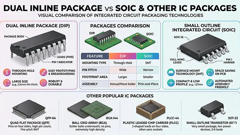
DIP vs SOIC
- DIP (Dual Inline Package): It have two parallel rows of pins for through-hole mounting. Supports socketing and breadboarding. DIP packaged components are ideal for beginners, repair, and rapid prototyping.
- SOIC (Small Outline IC): A surface-mount (SMD) IC with “gull-wing” leads bent outward. SOIC (and SOP package) are designed for automatic machine placement and ultra-compact PCB layouts.
- DIP vs SOIC: DIP packages typically occupy more PCB area and are taller, while SOIC/SOP packages can save board space but may affect maintainability for users.
Table: Comparing DIP, SOIC, SOP
| Attribute | DIP (PDIP, CDIP) | SOIC / SOP Package |
| Mounting | Through-hole | Surface-mount |
| Component Replacement | Easy (socketed/swapped) | Difficult/manual rework required |
| Prototyping | Breadboard-friendly | Needs adapter/breakout |
| Number of Pins | 8–64 (even number) | Up to 56+ |
| Package Uses | Retro, education, repairs, protos | New compact products |
Applications of DIP: Where and Why DIP Technology is Used
Applications of DIP packaging span industries and decades.
Core Uses
- Microcontrollers & Programmable ICs: From Arduino’s ATmega328P to vintage Intel 8085, DIP makes firmware and circuit upgrad straightforward.
- Memory ICs: RAM, EPROMs, Flash in DIP, easily for computer upgrades or repairs.
- Logic, Analog, and Interface Chips: Gates, op-amps, voltage regulators, SOIC-difficult tasks like analog prototyping remain best in DIP.
- Switches, Displays, and Relays: DIP switch, seven-segment displays, and relay driver ICs all can be found in DIP.
Niche and Legacy DIP Applications
- Spacecraft and Military: Ceramic DIP packages are still chosen for ultra-high reliability and serviceability in critical systems.
- Industrial Automation and Medical Devices: DIP packaged components are still used in process controllers, legacy sensors, and diagnostic hardware due to their reliability, socket-compatibility, and the ongoing possibility of component replacement.
- Retro Computing & Hobby Electronics: The DIP and skinny dual in-line package formats allow restoration of classic devices and easy integration into custom builds or homebrew computers.
- Rapid Prototyping: DIPs remain the go-to for fast testing of integrated circuit designs on breadboards or stripboards.
- Field Engineering: In environments where field repairs or upgrades are needed, the dual inline package meaning becomes synonymous with quick interventions and extended product life.
Popular Applications of DIP Packages
| Application Area | DIP Component Examples | Reason for DIP Use |
| Embedded Microcontrollers | ATmega328P, PIC16F877 | Breadboard/prototyping; socket-install |
| Analog Signal Processing | LM324, TL071 (op-amps) | Reliable through-hole, educational use, easy upgrades |
| Digital Logic | 74HCxxx, 4000 series | Breadboard and legacy system compatibility |
| Legacy Computing | Z80, 6502 CPUs, EPROM/ROMs | Direct replacement, socket-swapping |
| Industrial/Medical | Relay drivers, signal ICs | Socketed for field service, robust against vibration |
| DIY Kits | Timers, counters, drivers | Universally compatible with standard PCB protos |
Advantages of DIP Packaging

These advantages have made DIP technology a good way of electronics engineers and enthusiasts for decades, it usually include high practicality and reliability:
- Simplicity of Installation: DIP packages is simply to handle the position, no matter soldering by hand or the automated wave soldering.
- Component Replacement: Replacing or upgrading DIP components is very simple, either directly on the circuit board or through plug-and-play connections.
- Robust Mechanical Support: The package body, with its two rows of parallel pins, provides robust mechanica stability for components on the printed circuit board (PCB).
- Compatibility with Educational and Prototyping Environments: The breadboard design is inherently compatible with DIP package dimensions, allow beginners&developers can quickly assemble debug circuits, making it easy to learn and efficient.
- Standardized Form Factor: Whether plastic or ceramic dual in-line packages, pin spacing and numbering rules are standard, ensuring cross-compatibility and interchangeability between products from different factorys.
- Thermal Performance (with ceramic DIP packages): Ideal for circuits that may cause high power or need environmental protection (in aerospace electronics).
- Legacy and Repair: Many DIPs have direct modern alternatives, it can decades-old systems in industry and research.
- Socket-Installable: DIP packaged components can be directly pluged into sockets without soldering, upgrades, or reuse, will make them suitable for prototyping or mission-critical equipment.
Cons of Dual Inline Packages
Every package form has trade-offs—here are the notable cons of dual inline packages:
- Space Requirements: The DIP package is more important than surface-mount alternatives, impacting miniaturiz or portable applications.
- Lower Packaging Density: Compared to SOIC or BGA, DIPs limit the number of connections per PCB area, it can let them less suitable for high-density logic.
- Manual Assembly Overhead: While install DIP packages by hand is great for prototyping, it’s less efficient for mass assembly of modern compact electronics, which favor SMT.
- Limited High-Frequency Performance: Longer DIP tins introduce higher capacitance, whom can make them less ideal for radio-frequency or high-speed board
- Mechanical Stress: Mechanically is stable, DIP pins can be bendr during handling, insertion, or extraction, and wide-body packages may be at higher risk during vibration.
- Cons of Dual Inline in Critical/Modern Designs: For the compact, wearable, or smartphone PCBs, DIP dimensions are easy too large.
Evolution of DIP Packaging: Past, Present, & Future
Past: DIP Origins and Standardization
- The history of dip packaging is marked by the move from hand-soldered, point-to-point wiring to reliable, scalable, and standardized structures on the PCB.
- The dual inline package meaning evolved as the default until the late 1980s, supporting everything from early digital watches to space-borne computers.
Present: DIP and SMT in Parallel
- The evolution of DIP packaging shows both persistence and adaptation.
- Products needing frequent in-field service, educational institutions, and legacy support continue to often use dip packaging, especially where the function of the DIP includes socketed replacement.
- SMT and SMD packages (SOIC, QFP, SOP package) decided bysize, wave soldering, and pick-and-place compatibility are very important.
Future: New Roles for DIP
- WithSMDs become smaller, the DIP packages shifts toward legacy, specialty, research prototypes, and open-source markets.
- Available in DIP: Many popular ICs are produced in both SMD (SOIC) and DIP to expanded its
- DIPs will remain important for STEM education, rapid new product proof-of-concept, and critical repairs where only hands and a soldering iron are available.
Frequently Asked Questions on Dual Inline Package Meaning
What does dual inline package mean?
It means a component package with two parallel rows of pins, which are inserted into holes on a PCB or a socket for both mechanical and electrical connection.
Why do DIP packages come in various materials like plastic and ceramic?
Plastic DIPs (PDIP)offers high cost-effectiveness and meet most consumer products; ceramic DIP (CDIP) providesthe environmental protection and heat dissipation, meeting the stringent requirements of industries such as aerospace and military.
How many pins does a DIP have?
DIP chips have different number of pins, it them highly versatile for different circuit designs.
What is the inside of the package like?
Inside the DIP is the silicon die (which is the brain of the IC), wire, a lead frame, and encapsulation with plastic or ceramic. This structure defends against moisture, mechanical shock, and protects the chip’s function.
When would you use a DIP over SOIC or SOP package?
When conducting prototype development, maintaining legacy systems, designing field-repairable equipment, DIP packages are the preferred choice; if a compact,mass-production board needs to be designed and surface mount technology (SMT) assembly tools are available, SOIC/SOP packages can be selected.
Can DIP packages be used in new designs?
Yes! While not common in mobile or high-density data applications, DIP packages are still popular for microcontroller projects, kits, industrial products, and rapid prototyping.
Conclusion: The Legacy and Ongoing Value of DIP Packages
The importance of dual in-line packages (DIPs) goes simple pin arrangement—they have long integrated into the underlying logic of engineering design, teaching, maintenance, and also innovative concepts. From early mainframes and home computers to today’s STEM classrooms and industrial equipment, DIP packaging has consistently represented the core characteristics of stability, reliability, clarity, intuitiveness, and ease of use.
- Structure of dip package: Sturdy, visible, and easy to inspect.
- Features of dual inline package: Iconic two parallel rows, standardized pins, compatibility with sockets and breadboards, high mechanical and electrical reliability.
- Advantages of dip: Repair-friendly, excellent for learning, and ideal for field upgrades or mods.
- Cons of dual inline: Larger footprint, limited for ultra-compact modern devices.
- Evolution of dip packaging: From mainframe, to microcontroller, to classroom, to repair bench—DIP has proven adaptable every step of the way.
So whether you’re buying new chips, building with DIP technology for a one-off project, or repairing a legacy system, knowing the dual inline package meaning gives you the know-how to select, install, and trust this time-tested package type.