
Introduction
At LHD TECH, we view NMOS transistor and PMOS transistor as the “muscles and nerves” of modern electronic systems—the fundamental executors of logic within microprocessors, memory chips, analog front-ends, and power ICs. As the two pillars of metal-oxide-semiconductor field-effect transistors(MOSFETs), these devices grant designers the precision to control the flow of current voltage; this capability is the deciding factor in realizing full-stack designs ranging from foundation for digital logic, power electronics, and analog circuit design.
We have repeatedly validated through our projects that the trade-offs involved in choice between NMOS and PMOS devices go beyond complementary behavior; these choices directly dictate switching speed, static and dynamic power consumption, and noise margins, and ultimately determine BOM costs and tape-out yields. In a typical CMOS inverter, the NMOS transistor pulls the output to a low level (ground) while the PMOS transistor pulls it to a high level (power rail)—a fundamental principle LHD TECH consistently upholds in its low-power, high-reliability designs. Factors such as current flow mobility differences (electrons vs. holes), process-induced threshold voltage drift, source and drain structure, gate voltage dependence, and I-V characteristics under varying load conditions—any deviation here can be amplified into a systemic risk during actual operation.
Therefore, in LHD TECH’s design process, we never view the choice one type of PMOS and NMOS transistors as a simple binary decision. Whether implementing pure NMOS logic, a pure PMOS pull-up array, or the mainstream complementary CMOS architecture, our engineers conduct a rigorous analysis: Is the gate drive voltage sufficient? Does the source-drain breakdown voltage provide adequate overshoot margin? Is the trade-off between on-resistance (Rds(on)) and gate charge (Qg) optimized for the switching frequency? These details ultimately determine the product’s stability across the -40°C to 125°C temperature range and dictate whether the customer’s system-level EMI/EMC compliance can be achieved.
The Fundamentals of NMOS and PMOS Transistors
What is an NMOS Transistor?
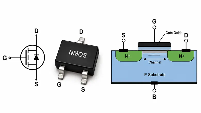
An NMOS transistor (n-channel metal-oxide-semiconductor field-effect transistor) is a type of MOSFET that utilizes an n-type doped region to form a conductive channel. Its source and drain consist of heavily doped n⁺ regions formed within a p-type semiconductor substrate. NMOS uses electrons as the primary charge carriers; since electron mobility in silicon is significantly higher than that of holes, NMOS transistors inherently exhibit faster switching speeds and lower on-resistance.
When a positive voltage is applied to the gate terminal, an electric field is induced beneath the gate oxide layer. Once the gate-source voltage VGS exceeds the threshold voltage Vth, this field causes inversion at the surface of the p-type substrate, creating an n-type conductive channel. allowing current to flow between the source and drain, placing the nmos transistor turns ON state.
It is precisely this high-speed, voltage-controlled switching capability that makes the NMOS transistors are fundamental components switching unit in digital integrated circuits, where it is widely employed in logic gates, memory cells, and high-speed signal paths. Practical applications require careful consideration of process-induced variations in threshold voltage, the body effect, and gate drive voltage margins to ensure reliable and consistent switching performance.
Key features of the NMOS transistor:
- Conducts current when positive gate voltage is applied
- Current flows from the drain to source
- NMOS transistors are extensively used in CPUs, memory cells, and digital logic circuits
- Working principles of NMOS: high mobility of electrons, low ON resistance, fast switching
- Structure of NMOS: n+ (source), gate (polysilicon or metal), n+ (drain), on p-type substrate
- NMOS transistor is similar to an electronic switch controlled by gate voltage
What is a PMOS Transistor?
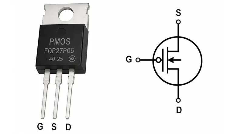
The PMOS transistor (p-channel MOSFET) is a core device within the MOS field-effect type of transistor family that complements the NMOS transistor. Structurally, PMOS transistors have p-type source and drain regions fabricated on an n-type semiconductor substrate. Conduction relies on holes—effectively positive charges resulting from the absence of electrons in the silicon lattice—as the primary charge carriers; since hole mobility is only about one-third that of electrons, the intrinsic switching speed of a PMOS transistor is generally lower than that of an NMOS transistor of comparable dimensions.
The conduction mechanism of a PMOS transistor is entirely complementary to that of an NMOS transistor: the device enters the conducting state only when the negative voltage is applied to the gate terminal. Specifically, when the pmos transistor turns ON when the gate voltage is low (i.e., more negative than the source), creating a p-type conductive channel; this allows holes to drift directionally flow between the source and drain, thereby establishing a current.
Key features of the PMOS transistor:
- PMOS uses holes as the main charge carrier
- Turns ON with negative gate voltage; gate voltage is low turns ON the PMOS
- Current flows from the source to drain
- PMOS transistors are integral to analog design, voltage regulation, and supply switching
- PMOS transistors act as high-side switches
- PMOS transistors are utilized in level shifters, analog current sources, and load circuits
- PMOS transistor symbol: arrow pointing outward (representing positive charge carrier flow)
NMOS and PMOS: The Two Main Types of MOS Transistors
MOSFETs fall into two main categories based on the primary charge carriers involved: NMOS and PMOS. One relies on the movement of electrons, while the other relies on the movement of holes. Regardless of the type, the structures of NMOS transistor and PMOS transistor are identical; both feature four terminals known as the gate, source, drain, and body. Applying a voltage to the gate allows the transistor to switch between ON and OFF states—acting like a switch to controlling the flow of current—where it conducts electricity when transistor turned on and blocks the flow when turned off.
Types of MOS transistors:
| Type | Channel Type | Charge Carrier | Source/Drain Type |
| N-channel (NMOS) | n-type | electrons | n+ (source/drain) |
| P-channel (PMOS) | p-type | holes | p+ (source/drain) |
Charge Carriers: Electrons vs. Holes
The charge carriers determine how easily current can flow between the source and drain.
In short, charge carriers determine how smoothly and quickly current flows between the source and the drain.
- In NMOS transistor operation, applying a gate voltage draws electrons into the channel, creating a highly conductive path. Conductivity of the transistor is excellent due to the fact that electrons move rapidly—meaning they have high mobility.
- In PMOS transistors, a sufficiently negative gate voltage is required to “pull” holes out and get them moving.
Compared to NMOS, PMOS devices typically exhibit higher resistance and slower response times, as holes do not move as nimbly as electrons.
Source and Drain: Structure and Current Flow
In the design of nmos transistor and pmos transistor , both the source and drain are heavily doped regions (n⁺ for NMOS, p⁺ for PMOS); one acts to “emit” charge carriers while the other “collects” them, enabling current flow. The specific direction and nature of the current flow depend entirely on the polarity of the gate voltage—different gate voltage polarities result in completely opposite conduction mechanisms.
- NMOS: When a positive gate voltage is applied, the surface of the p-type substrate beneath the gate undergoes inversion to form an n-type channel. This effectively creates a dedicated path for electrons, allowing them to flow smoothly from the source to the drain.
- PMOS: Here, a negative voltage is applied to the gate terminal. This negative voltage attracts holes to form a p-type channel, allowing current to flow between the source(p⁺ region) and the drain (p⁺ region)—though in this case, the current travels through the n-type substrate.
Structural and Symbolic Differences
Structure of NMOS
NMOS—AnNMOS transistor consists of a p-type substrate, an insulated gate (typically made of polysilicon), and n⁺ source and drain regions. When the gate voltage is high, electrons accumulate beneath the gate, allowing current to flow between the source and drain. This embodies the essence of the field-effect transistor: using an electric field (applied to the gate) to enable or cut off the current path.
Structure of PMOS
PMOS—This type features an n-type substrate combined with p⁺ source and drain regions. When a negative voltage is applied to the gate, holes accumulate beneath the gate to form a p-type channel, thereby allowing current to flow between the source and drain.
Differences between PMOS and NMOS:
| Feature | NMOS | PMOS |
| Main Carrier | Electrons | Holes |
| Substrate | P-type | N-type |
| Source/Drain | N+ | P+ |
| Symbol Arrow | Inward (toward gate/body) | Outward (from gate/body) |
| Gate ON Voltage | Positive (V<sub>GS</sub> > V<sub>th</sub>) | Negative (V<sub>GS</sub> < V<sub>th</sub>) |
| Current Flow | Drain → Source | Source → Drain |
| ON Resistance | Lower (compared to PMOS) | Higher |
| Mobility | Higher (electrons) | Lower (holes) |
| Typical use | Pull-down, digital, logic gates | Pull-up, analog, high-side switches |
Operating Principles: How NMOS and PMOS Work
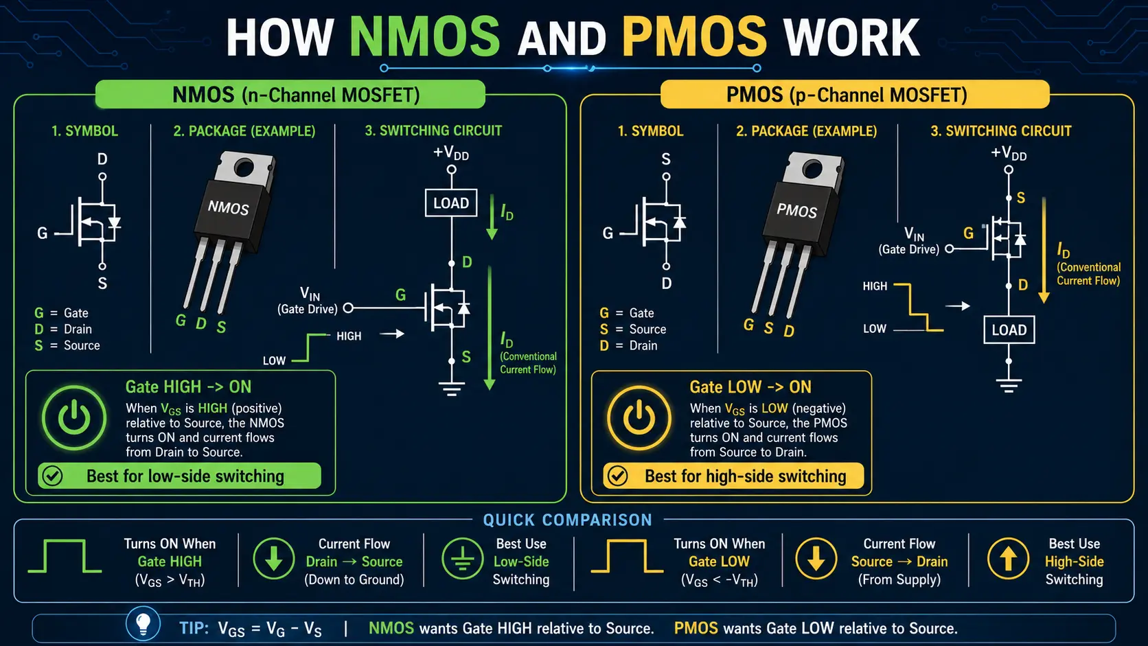
Understanding how NMOS and PMOS transistors conduct current is vital for robust circuit design:
NMOS Transistor Work
- When a positive voltage exceeding the threshold voltage is applied to the gate, an electric field forms across the gate oxide. This field pulls electrons into the channel beneath the gate, allowing current flow.
- If the voltage applied to the gate is below the threshold voltage, an inversion layer does not form on the substrate surface, and no channel is created; consequently, the transistor remains in the off state, blocking current flow.
- while we describe current flows from the drain to the source, the actual charge carriers—the electrons—move physically from the source to the drain.
- NMOS transistors conduct current efficiently, making them the standard choice for digital logic paths that demand high speed.
PMOS Transistor Work
- For a PMOS transistor to conduct, a negative voltage is applied to the gate relative to the source. This negative gate voltage attracts holes—the majority carriers in a PMOS device—forming a conductive channel beneath the gate.
- PMOS transistors conduct the gate potential to be more negative than the source potential; this allows holes to move from the source to the drain, enabling current flow.
- If the gate voltage is high level (close to the supply voltage), the channel cannot form, and the transistor remains in the off state, preventing current flow.
Field-Effect and Gate Voltage Control
Both NMOS and PMOS transistors are field-effect devices, meaning voltage to the gate (not current) controls the conductivity of the channel, affecting whether the transistor is ON or OFF. This property is what makes them so energy efficient.
- Transistor turns ON: Sufficient gate voltage triggers conduction.
- Transistor operation is fully voltage-controlled, minimizing steady-state power.
The Body Effect in MOSFETs
The threshold voltage of both nmos transistor and pmos transistor is not entirely fixed; it can be shifted by the potential across the source and substrate (“body”) terminals—a phenomenon called the body effect. This can alter transistor operation in large ICs, especially if the source is not at the same voltage as the substrate.
Key Differences: Extended Comparison Table
| Parameter | NMOS Transistor | PMOS Transistor |
| Channel type | N-channel | P-channel |
| Main charge carrier | Electrons | Holes |
| Substrate type | P-type | N-type |
| Source and drain type | N+ | P+ |
| Gate voltage ON | Positive | Negative |
| Gate voltage OFF | Zero or negative | Zero or positive |
| Current flow | Drain to source (electrons: S → D) | Source to drain (holes: S → D) |
| Current between the source | Flow reversed compared to PMOS | Flow reversed compared to NMOS |
| Mobility and speed | Higher | Lower |
| Resistance | Lower | Higher |
| Power consumption | Lower in active, scalable | Typically higher in high-speed |
| Fabrication size | Smaller for same ON resistance | Must be wider for same R<sub>ON</sub> |
| Symbol arrow | Inward | Outward |
| Typical use-case | Pull-down, logic | Pull-up, high-side switching |
Performance, Efficiency, and Design Tips
Why NMOS Transistors are Extensively Used
- NMOS transistors operate faster and require less area for a given ON resistance.
- NMOS transistors in a complementary MOS (CMOS) configuration provide quick discharge paths in logic.
- Compared to PMOS transistors, NMOS are better for speed, but both are critical for noise immunity and efficiency in CMOS.
Why PMOS Transistors are Integral
- PMOS transistors are typically used for high-side switching.
- PMOS transistors are often used in power management (load switches, battery disconnects).
- PMOS transistors exhibit better noise immunity when used as pull-up devices.
- PMOS transistors are commonly used in analog loads due to their stable behavior and as part of current mirrors.
Choosing Between NMOS and PMOS
The choice between nmos and pmos depends on the circuit:
- Use NMOS for speed, ground-referenced switching, and compact logic.
- Use PMOS for high-side switching, analog current sources, and voltage-level shifting.
PMOS and NMOS transistors are essential in tandem for robust digital logic:
- CMOS technology combines both pmos and nmos for ultra-low static power and excellent logic margins.
Applications, Circuit Examples, and Advanced Design
NMOS and PMOS in Practice
Transistors are commonly used in the following ways:
- NMOS transistor: Digital logic, microprocessors, pull-down in logic gates, boost/fly back switching regulators (as low-side switch).
- PMOS transistor: Load switches, battery management, analog current mirrors, voltage level shifters, pull-up parts of logic.
Working Principles of NMOS enable its use in:
- Fast digital circuits: SRAM, FIFO buffers, high-speed buses.
- CMOS logic gates: as the “pull-down” partner.
Example: Logic Gate Operation
CMOS Inverter
- NMOS and PMOS transistors in a complementary arrangement:
- Input = LOW: PMOS ON (output pulled to supply voltage), NMOS OFF.
- Input = HIGH: NMOS ON (output pulled to ground), PMOS OFF.
This complementary behavior of PMOS and NMOS cancels static current flow—only switch events consume power.
CMOS Technology: The Power of Complementary NMOS and PMOS
The greatest efficiency comes from nmos and pmos transistors working together in complementary MOS (CMOS):
- CMOS gates consume almost no static power.
- Combines both pmos and nmos for balanced drive strength and sharp transitions.
- Found in every microcontroller, processor, and digital IC.
Behavior of PMOS and NMOS in CMOS allows reliable, scalable logic.
Challenges, Reliability, and Future Trends
- As device geometries shrink, controlling threshold voltage, leakage, and body effect is critical.
- Tips: Use multi-threshold CMOS, power gating, and voltage regulation strategies for low standby power.
- Current research in silicon-on-insulator and high-mobility materials aims to address the difference between NMOS and PMOS performance as Moore’s Law continues.
FAQs About NMOS vs PMOS
1. What is the main difference between NMOS and PMOS?
NMOS uses electrons as its primary charge carriers, while PMOS uses holes. NMOS turns on with a positive gate-to-source voltage, whereas PMOS turns on when its gate voltage is lower than its source voltage.
2. How do NMOS and PMOS transistors work?
An NMOS conducts when its gate voltage exceeds its source voltage by the threshold voltage. A PMOS conducts when its source voltage is sufficiently higher than its gate voltage.
3. What is the difference between NMOS and PMOS symbols?
NMOS and PMOS symbols use opposite body or source-arrow directions. PMOS logic symbols may also include a gate bubble to indicate that the transistor is activated by a low gate voltage.
4. How can you tell whether a MOSFET is NMOS or PMOS?
Check the part number and datasheet first. The circuit connection also provides a clue: NMOS is commonly connected toward ground, while PMOS is often connected toward the positive supply rail.
5. Why is NMOS generally faster than PMOS?
Electrons have higher mobility than holes, allowing NMOS transistors to conduct more current for the same device size. This generally gives NMOS lower resistance and faster switching performance.
6. Why is PMOS usually larger than NMOS?
PMOS devices are often made wider to compensate for the lower mobility of holes. The larger channel helps PMOS deliver current comparable to an NMOS transistor in CMOS circuits.
7. Why does NMOS pass a strong 0 but a weak 1?
NMOS can pull an output close to ground without significant voltage loss. When passing a high level, the output is limited to approximately the gate voltage minus the threshold voltage.
8. Why does PMOS pass a strong 1 but a weak 0?
PMOS can pull an output close to the positive supply voltage. However, when passing a low level, its threshold voltage prevents the output from reaching ground completely.
9. Why are PMOS and NMOS used as pull-up and pull-down transistors?
PMOS efficiently connects an output to VDD, making it suitable for pull-up networks. NMOS efficiently connects an output to ground, making it suitable for pull-down networks.
10. Which is better, NMOS or PMOS?
Neither is universally better. NMOS is preferred for fast, efficient low-side switching, while PMOS simplifies high-side switching. The best choice depends on voltage, current, speed, and gate-drive requirements.
Conclusion, Tips, and Resources
NMOS and PMOS transistors are the cornerstones of the digital world. Their structure, transistor operation, charge carrier type, source and drain connections, and gate voltage control shape logic, analog, and power circuits at every level of integration.
- NMOS transistor: Turns ON when a positive voltage is applied to the gate, has higher speed, lower ON-resistance, and is used in high-frequency and digital applications.
- PMOS transistor: Turns ON when a negative voltage is applied to the gate, is robust for high-side switching, voltage control, and analog loads.
- PMOS uses holes, while NMOS uses electrons—this difference in charge carrier affects the mobility, ON-resistance, speed, and design strategies of each device.
- The nuanced difference between NMOS and PMOS is at the heart of circuit design, from logic gates to advanced power management ICs.
Design Checklist and Tips
- In digital CMOS, always pair nmos and pmos for optimal power and performance.
- For high-side load switches, choose PMOS; for low-side, use NMOS.
- Pay close attention to threshold voltage and body effect—these impact reliability and switching margins.
- When you need to control the flow of current dynamically with voltage and not current, use a MOSFET rather than a bipolar transistor.
- Use simulators to see the impact of gate voltage, threshold voltage, and source/drain bias on transistor performance.
Final Perspective
The behavior of PMOS and NMOS—their response to gate voltage, applied to the gate, and current flow paths—makes them not only the building blocks of digital logic but the fine-tuners of analog performance and power efficiency in almost every electronic device you use.