

Introduction to PCB Routing

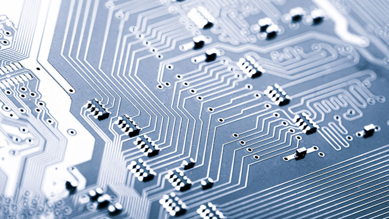
PCB routing refers to the process of planning conductive paths on a printed circuit board (PCB). These paths, also known as traces, are responsible for connecting various electronic components and ensuring the stable operation of the circuit. Upon completion of schematic capture, the design proceeds to the placement phase, where it is necessary to efficiently plan the routing of signal, power and ground lines. A well-designed routing scheme can improve the overall quality and performance of the circuit board, which is specifically reflected in reducing signal distortion, preserving signal integrity, while optimizing the design’s manufacturability and enhancing its operational efficiency.
PCB routing involves multiple critical variables, including component placement and trace planning, trace width settings, trace clearance control, and return path design. For high-speed complex circuits, routing must also pay special attention to maintaining signal integrity. Each trace and via directly impacts the electrical characteristics of the circuit, making mastery of efficient PCB routing techniques an essential foundation for achieving optimal circuit performance.
PCB Routing Basics

PCB routing begins with the transformation of the schematic into a pcb layout. This stage converts netlists (logical connections) into physical copper pathways that control the flow of current and signal through a printed circuit board. Let’s review the heart of this process:
Key Elements of PCB Routing:
- Traces:The conductive pathways that connect pins and pads on components; they dictate how signals and power travel across the board.
- Vias:Metallized holes that allow traces to jump between layers—especially important in multilayer routing.
- Pads:Areas of copper connected to component leads and pins.
PCB routing strategies involve:
- Routing signals with the shortest paths to reduce resistance, inductance and potential for noise pickup.
- Using routing strategies that isolate high-speed traces and sensitive analog areas from noisy digital sections.
- Applying pcb routing guidelines for trace width, clearance and return path management.
The Role of PCB Routing in Signal Integrity
In PCB routing design, maintaining the integrity of signal transmission is a core objective. Signal integrity is specifically characterized by the quality and stability exhibited by electrical signals as they propagate through PCB traces. A PCB routing scheme exerts a direct influence on signal quality and this conclusion applies to both analog and digital circuit scenarios.
Why is signal integrity important?
- High-speed digital circuits are prone to signal degradation, reflections and noise if traces are poorly routed.
- Analog circuits require clean, low-noise signal paths to function optimally.
- Impedance mismatches and excessive via usage can introduce reflections, delay and loss of data—especially in differential and high-speed applications.
Improper routing can lead to a range of issues such as data errors, EMI emissions, timing disorders, and ultimately result in the overall degradation of circuit performance.
Key PCB Routing Strategies and Techniques
Fundamental Routing Strategies
- Shortest Path:Always route the shortest, most direct path between components to minimize resistance and signal delay.
- Orthogonal Routing:Arrange traces on adjacent layers to run at 90-degree angles (orthogonally) to minimize crosstalk and noise.
- Keep High-Speed and Analog Separate:Use routing to physically isolate noisy signals from sensitive sections.
- Manual Routing for Critical Signals:While autorouters are fast, manual routing (interactive routing) for clocks, differential pairs and critical nets achieves higher quality and optimal circuit performance.
- Bus Routing:Carefully space parallel buses like data/address lines; match their trace lengths to avoid skew.
Common Routing Features and Their Impact
| Routing Feature | Impact on Signal & Power |
| Short, Wide Traces | Lower resistance, less voltage drop |
| Fewer Vias | Less capacitance/inductance added |
| Continuous Ground Plane | Better return path & signal shielding |
| Controlled Impedance | Reduced signal reflection |
Optimal Component Placement and Routing
Effective component placement and routing is the foundation for all routing decisions and optimal circuit performance.
- Group Related Components:Minimize trace length and routing complexity.
- Input/Output Near Edges:Place connectors and high-pin-count components near the board edge for accessibility.
- Keep Decoupling Caps Close:Place power decoupling caps close to IC pins to minimize loops (and EM emissions).
- Leave Room for Routing:Avoid overpacking components—leave adequate space for routing pcb traces and placing vias.
Power and Ground Routing
Routing power and ground is as critical as signal paths:
- Wide Traces/Pours:Use wider power and ground traces or pours to reduce resistance, heat and voltage sag.
- Dedicated Power/Ground Planes:In multilayer designs, reserve whole layers for power and ground, which dramatically improves power delivery and provides a clean return path for signals.
- Stitching Vias:For wide traces and polygons, use “stitching” vias to connect multiple layers and further reduce impedance.
Recommended Minimum Trace Width (per IPC-2221)
| Trace Current | Min. Trace Width (1oz Cu) | Use Case |
| 0.5A | 0.25 mm | Logic, low-power |
| 2A | 1 mm | Power, relays, etc. |
| 5A | 2.5 mm | Motors, high-power |
Advanced PCB Routing Concepts
As boards become smaller and circuits run faster, advanced routing is required:
- High-Speed Signal Traces:Use controlled impedance and match trace lengths to prevent skew and data loss.
- Differential Pairs:Always route differential pairs together with matched length and spacing.
- Return Path Management:Ensure every high-speed signal has a low-inductance, unbroken return path (typically underneath the trace on a ground plane).
Impedance and Controlled Impedance Routing
Impedance routing refers to the practice of designing traces with a precise impedance—in most digital designs, typically 50Ω.
- Why it Matters:Impedance mismatches can cause reflections that corrupt data, especially above 100 MHz.
- How to Achieve Controlled Impedance:Use the correct trace geometry, spacing from the reference plane (usually ground), and consistent width, aided by PCB design software calculators.
Effective routing for impedance:
- Place critical high-speed traces over continuous ground planes.
- Avoid abrupt changes in width or stubs that act as antennas.
Multilayer Routing for Complex Designs

Multilayer routing forms the core technical foundation for the design of complex printed circuit boards (PCBs). This technology is of particular importance for scenarios involving high-density component placement and high-speed signal transmission. By leveraging two or more copper foil layers, designers can devise more sophisticated routing schemes, which achieve physical isolation of high-speed signal channels, high-current transmission paths and sensitive signal traces. These layout practices directly enhance the utilization rate of routing space on the circuit board and simultaneously facilitate the optimization of the circuit’s overall performance metrics.
Key Advantages of Multilayer Routing
- Greater Routing Density:More layers mean more space to route traces, reducing overlap and potential for crosstalk.
- Dedicated Planes:Middle layers often serve solely as solid ground or power planes, ensuring a low-impedance return path which is crucial to maintain signal integrity and improve electromagnetic compatibility.
- Improved Signal and Power Integrity:Shorter, more direct return paths for high-speed signal traces and minimized noise coupling, resulting in more robust and efficient PCB designs.
- Effective Routing for Advanced Designs:With multiple layers, designers can apply advanced PCB routing strategies such as orthogonal routing on adjacent layers and through-via signal transitions that optimize layout for both manufacturability and performance.
Four-Layer Stackup
| Layer | Common Use |
| 1 | Signal/Components |
| 2 | Ground Plane (return path for signals) |
| 3 | Power Plane (stable distribution) |
| 4 | Signal |
PCB Layout and Efficient PCB Design
An efficient printed circuit board design commences with a layout scheme that is logically coherent and thoroughly planned. The layout scheme directly determines the specific performance of electrical parameters. It profoundly influences the manufacturability of the production process. The scheme is also integral to overall project cost control. The quality level of the final product is fundamentally shaped by the layout scheme.
Principles of Efficient PCB Design
- Minimize Trace Lengths:Shorter traces reduce losses, minimize signal distortion and lower electromagnetic emissions.
- Route Signals Regularly:Avoid sharp angles and convoluted paths. Use 45° bends instead of 90° to reduce signal reflections—an essential aspect of effective routing.
- Space for Inspection and Testing:Leave sufficient access for probing signals during pcb assembly and troubleshooting.
Best Practices for PCB Layout
- Symmetry:Symmetrical placement promotes even signal and power distribution, enhancing performance and reliability.
- Component Orientation:Uniform orientation minimizes routing complexity and reduces the likelihood of assembly errors.
- Avoiding Inadequate Routing:Poorly routed boards can suffer from open/short circuits, excessive EMI, overheating or even total failure—highlighting why pcb routing is essential and not just a cosmetic phase of design.
Common Routing Mistakes and How to Avoid Them
Even experienced designers face the potential risks of these common design pitfalls. Establishing standardized workflows and strictly adhering to industry best practices serve as effective preventive measures. Such standards systematically reduce the occurrence probability of critical design errors. This preventive approach ultimately minimizes the financial and time losses that a project may incur.
Common Mistakes in PCB Routing
- Ignoring Return Paths:Failing to provide a clear, direct return path can introduce noise and degrade signal integrity.
- Excessive Use of Vias:Each via adds inductance and resistance; overuse can harm both signal and power distribution.
- Insufficient Trace Clearance:Violating design rules for minimum spacing leads to shorts or arcing, especially in high-voltage applications.
- Narrow Power and Ground Traces:Results in voltage drop and possible overheating—routing power and ground efficiently is crucial.
- Inconsistent Trace Widths:Leads to impedance mismatches and unreliable performance across similar signals.
Poor routing practices can give rise to multiple technical issues. Signal transmission may experience data corruption. Insufficient heat dissipation will lead to thermal failure. Designs may fail compliance testing. Severe routing flaws can also cause physical damage to circuit boards.
Tips for Optimizing PCB Routing

Poor routing practices give rise to a series of technical issues. Signal transmission may suffer from data corruption. Inadequate heat dissipation leads to thermal failure. Design outcomes might fail compliance testing. Severe routing flaws can result in physical damage to circuit boards.
Top Tips for Optimizing PCB Routing
- Start with a Clean Netlist:Ensure schematic wiring matches intended connections.
- Prioritize Critical Nets:Route high-speed signals and clocks first, minimizing their length and avoiding noisy sections.
- Keep Return Paths Short:Route signals over continuous ground planes to both ensure signal and power integrity and minimize signal distortion.
- Group Related Routing:Bundle related signals (such as buses) together for matched electrical length.
- Use Interactive Routing Features:Modern pcb design software includes interactive routing, push-and-shove routing, and real-time DRC—leverage these for efficient PCB.
- Double-Check with Simulation:Tools for signal and power integrity help identify potential issues before manufacturing.
- Regular DRC Checks:Run automated checks after each routing session to spot clearance, width or stubs.
- Consult the Manufacturer:When in doubt, ask your PCB fabricator for their best practices—especially for advanced stackups or processes.
Effective PCB Routing Techniques for High-Speed and Power Integrity
High-speed routing introduces new challenges: the risk of signal degradation, electromagnetic emissions and timing failures rises as circuit speeds increase.
Effective Techniques
- Controlled Impedance Traces:Calculate trace width and height for the target impedance (commonly 50 or 100 ohms) using the board’s dielectric and stackup.
- Differential Routing:Keep differential pairs tightly coupled; run with matched lengths and spacing through all layer transitions.
- Minimize Parallel Runs:Parallel traces couple capacitively, risking crosstalk. Separate sensitive signals and use ground traces as guards where needed.
- Limit Stub Lengths:Stubs (dead-end trace pieces) can act as reflection points; eliminate or keep them extremely short.
Practical Power Integrity Tactics
- Decoupling Networks:Use multiple capacitors (distributed across frequency ranges) close to each IC’s power pins.
- Wider Power Planes:Carry high current with minimal voltage drop using polygons or dedicated planes, stitched with multiple vias for low impedance.
The Role of PCB Design Software and Interactive Routing
Modern PCB design software—such as Altium Designer, KiCad and Cadence Allegro—is vital to both manual routing and advanced, interactive routing strategies.
Key Routing Features in PCB Design Software
- Design Rule Integration:Enforces spacing, clearance and width rules in real-time.
- Push-and-Shove Routing:Allows existing traces to move dynamically, making dense routing areas manageable.
- Differential/Impedance Pair Managers:Automate rules and length tuning for controlled impedance and differential pair signals.
- Real-Time DRC and ERC:Automatic flagging of errors ensures high quality of PCB before sign-off.
- Visualization Tools:3D view, net highlighting and layer stack analysis help in identifying hidden issues and optimizing routing decisions.
Manual Routing vs. Autorouting
While auto-routing is fast and useful for generic connections or low-speed signals, manual routing is still crucial for all high-speed, impedance-controlled and critical signal paths. The best boards are often created by combining both, using interactive features for high-density sections.
FAQs about PCB Routing
Q: Why is PCB routing important in the design process?
A: PCB routing is essential because it directly affects electrical performance, manufacturability, and long-term reliability. Good routing strategies enable effective layout, minimal signal distortion and robust operation.
Q: What are controlled impedance traces?
A: These are traces designed with specific width, spacing and distance from ground planes to achieve a set electrical impedance—critical for high-speed digital and RF signals.
Q: How does inadequate routing impact circuit performance?
A: Inadequate routing can introduce impedance mismatch, excessive noise, return path disruptions and even outright circuit failure. It can cause data corruption, EMI failures and overheating.
Q: What are the best practices for routing power and ground traces?
A: Use wide traces or dedicated planes, keep current loops short and use stitching vias to lower impedance.
Q: How do you minimize crosstalk and electromagnetic emissions?
A: Use solid ground planes, avoid parallel routing for sensitive signals, apply adequate spacing and shield key nets with ground or power pours.
Conclusion: Why PCB Routing is Essential to Optimal Circuit Performance
PCB routing plays an absolutely central role in every aspect of pcb design. The difference between a stable circuit and one that fails in the field often comes down to the skill applied in the routing phase. Effective PCB routing techniques boost quality, ensure signal and power integrity, reduce electromagnetic emissions and ensure manufacturability.
In the end, pcb routing enhances every stage of the hardware journey—from layout to fielded product. Applying pcb routing strategies such as optimal component placement, careful power/ground routing and attention to controlled impedance ensures not just a working design, but one that stands up to every practical challenge.
PCB routing is the process where theoretical schematics become reliable, manufacturable and efficient circuits. Make every routing decision count, leverage modern pcb design software and never hesitate to iterate and improve. By mastering these strategies, you ensure that your designs aren’t just functional—they’re truly world class.