
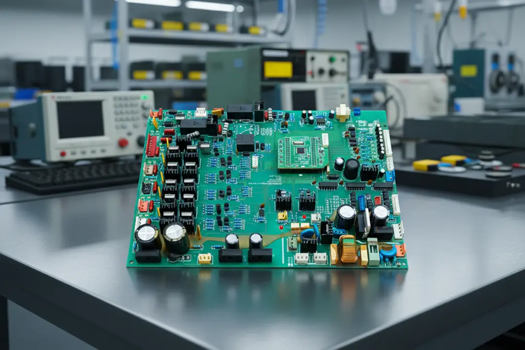
Introduction: The Heart of IoT—PCB Design and Circuit Boards
In today rapidly advancing digital world, the internet of things (IoT) is transform everyday environment. The heartbeat of every IoT devices is its circuit board—specifically, expert craft printed circuit boards that determine how sensor, communication modules, and processors interact. PCB design for IoT is not just about connecting components; it’s about optimizing each element for reliability, low power consumption, advanced communication, and long-term sustainability.
IoT devices often operate at the edge, sometime in remote location or wearable format, and are task with real-time data collection, control, and communication with other devices or the internet without the need for human intervention. This meaning every decision around pcb design, circuit board layout, andelectronic components affects the overall device performance and its ability to operate for extend periods without frequent maintenance or power replacement.
PCB Design for IoT Device Functionality
The function of IoT device relies heavily on robust pcb design for iot. IoT devices often blend sens, process, and communicate, demand that each board made must be fit for specific function and environment.
Essential Capabilities of IoT Devices
- Sensing the Environment: Integration of temperature, humidity, motion, or gas sensor to gather real-world data.
- Data Processing: Embed micro-controllers or microprocessors interpret sensor signals inside the circuit.
- Wireless Communication: IoT device rely on wireless communication protocol like Bluetooth, Wi-Fi, Zigbee, LoRa, and cellular to share data with other device or the cloud.
- Automation and Remote Control: Actuators on the circuit board enable smart lock, smart light, and automation without human help.
Why PCB Design is the Choice for IoT
- Size Optimization: Device often need to be compacted, wearable, or unobtrusive, with small, densely populated boards for IoT applications.
- Low Power Consumption: Ensure optimal energy consumption is critical as most IoT devices operate on battery power.
- Long-Term Reliability: IoT PCBs must withstand harsh environment (humidity, dust, vibration, temperature extremes) and operate for extend periods without frequent servicing.
Efficient IoT: Optimizing PCB Design for Connectivity and Low Power
Optimizing Boards for IoT Connectivity
- High-Quality Antenna Performance: Ensure the device can communicate with other devices or the internet efficient.
- Signal Integrity: Proper circuit design and rout of traces for power lines and signal traces optimize signal integrity. Shielding sensitive areas is integral in minimize electromagnetic interference.
- Design for Modular Communication: Use sockets or connectors for upgradeable wireless modules (for future-proofing and flexibility).
Achieving Low Power Consumption
- Component Selection: Use low power MCUs, efficient voltage regulators, and energy-saving sensors early in the design process.
- Design Techniques: Employ power-gating, deep sleep modes, and energy harvest for wearable devices or remote node.
- Optimal PCB Size and Layering: Shrink the board size without compromise performance, and using multi-layer designs to isolate power, signals, and ground to reduce losses.
Applications of IoT: How Circuit Design Powers Modern Life
The wide spectrum of application of IoT is possible thank to innovation in pcb design and manufacture.
Examples of IoT Applications
| Application | Description | IoT Device Example | Specific Circuit Board Features |
| Smart Home Automation | Automates light, security, HVAC | Smart thermostat, wi-fi lock | Multi-protocol radio, low power, compact PCB |
| Industrial IoT (IIoT) | Monitors equipment, automation systems | Vibration monitor, asset tracker | Rugged, shielded, multi-layer circuit |
| Healthcare & Wearables | Personal monitoring, real-time diagnostic | Smart watch, biosensor patch | Flexible pcb, biocompatible, ultralow power |
| Smart Agriculture | Remote field/ocean/soil sensor | Soil moisture probe, livestock tracker | LoRa, solar harvester, water-proofed board |
| Smart Utility | Monitors and automates meters, infrastructure | NB-IoT water meter | Secure element, robust isolation, compact PCB |
| Connect Transport | Asset and fleet monitoring, predictive maintenance | Fleet tracker, OBD device | Cellular, GPS, automotive-grade component |
Boards for IoT: Components, Materials, and Communication
Efficient boards for IoT require carefully integration of additional component, material selection, and communication modules to ensure optimal performance and durability.
Key Electronic Components in IoT Boards
- Micro–controllers (MCUs): Atmel/Microchip ARM Cortex-M, ESP32, STM32, and similar low-power processors.
- Sensors: For temperature, humidity, gas, motion, and more.
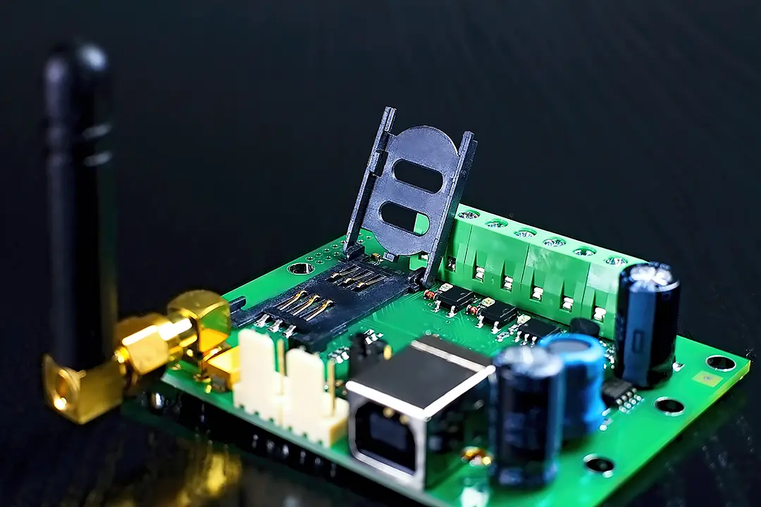
- Wireless Modules: BLE, Wi-Fi, Zigbee, LoRa, and LTE-M for fast, reliable wireless communicate.
- Power Management: Efficient voltage regulator, buck/boost converters, supercaps for stable operation.
- Flash Memory: For firmware, logs, and supporting OTA updates.
- Antenna: Careful placed, tuned, and isolated for high radio efficiency.
Common PCB Materials for IoT
- FR-4: General-purpose, cost-effective, up to moderate frequency circuits.
- Polyimide: For flexible boards in wearable and robotics.
- Ceramic/Metal-core: Used in high-heat or high-frequency applications for better heat dissipation or RF performance.
Communication and Automation
- IoT devices often must communication with other devices, support automation, and enable real-time response through robust and flexible PCB communicate pathways.
Circuit Design Techniques for IoT Boards
IoT circuit design involve a blend of fundamentals and cutting-edge techniques geared towards maximizing performance, lower power, and ensuring reliability.
Best Practices
- Early in the Design Process: Identify all system requirement—connectivity, power, sensor types, and physical constraint.
- Signal Traces and Rout: Short, impedance-match, and shield traces for high-speed or RF signals to optimize signal integrity.
- EMI & Electromagnetic Interference Mitigation: Ground planes and careful trace separation to reduce electromagnetic noise.
- Component Placement: Place high-frequency or noise-sensitive component far from antenna and using dedicate layers for power and ground.
Design for Quality Control & Testing
- Include test points and debug headers for quality control.
- Design potential expansion or upgrade options, allowing boards for IoT to evolve as application demands change.
PCB Design and Manufacturing for IoT Devices
PCB design and manufacturing are critical in deliver high-performance IoT boards. Specialized processes and quality control measures ensure boards operate effectively in the real world.
PCB Manufacturing Considerations
- Panelization for Efficient Assembly: Allow multiple boards made in one manufacture
- Surface Finishes: ENIG, OSP, or hard gold for corrosion resistance and longevity, make sure each board made for IoT are suitable for extended periods without frequent maintenance.
- SMT vs. Through-Hole Technologies: Most IoT design use SMT for space efficiency and scalability, while through-hole mounts are reserved for connectors or component require mechanical robustness.
- Quality Control Measures:
- In-circuit test and automat optical inspection to ensure optimal placement and solder joint quality.
- Environmental stress screenedto verify boards for IoT maintain reliability under real-world conditions.
- X-ray inspection for detect hidden solder defects, especial in dense multi-layer IoT board.
Optimizing IoT Boards for Reliability, Low Power, and Performance
Ensure optimal operation for IoT device mean careful optimization throughout the design processing.
Reliability
- Redundant Power Paths: For critical application, design alternate trace for power line or dual power source (primary and backup battery).
- Component De-rating: Running all component significantly below their maximum rat for enhanced longevity—a crucial strategy for IoT device that must operate for extend period without frequent field maintenance.
- Conformal Coating and Potting: Selective coat or full pot protects sensitive circuit board from dust, moisture, vibration, and chemical exposure.
Low Power Optimization
- Power Domains: Dividing the circuit into power domain so only essential parts are energize at a time. Using additional component likely digital load switches or power-gating FETs.
- Energy Harvesting: Integrated ambient energy capture (solar, thermoelectric, RF) can extend device life or even eliminate the need for manual battery replacement in some IoT project.
- Dynamic Power Scaling: Use firmware to adjust processor clock rate and selective power down high-draw peripherals between task.
Ensuring Board Performs Optimally
- Optimizing Signal Integrity: Through control impedance rout, differential pair layout for high-speed bus, and robust ground plane, IoT PCBs can avoid electromagnetic interference and guarantee reliable data transmission.
- Antenna Performance: Ensuring antenna isolation from heat-producing or noisy digital circuits to maximize range and communication quality—antenna placement is often the most critical part of communication modules in compact device.
Quick Reference: IoT Board Optimization Checklist
| Optimization Area | Best Practice |
| Low Power | Deep sleep modes, efficient voltage regulators, energy harvesting |
| Reliability | Quality control, de-rating, protective coatings |
| Connectivity | Optimized antenna layout, modular radios |
| Signal Integrity | Controlled impedance, filtered supply rails |
| Manufacturing | DFM review, traceability, environmental stress tests |
Case Study: Circuit Board Solutions in IoT Applications
Let’s see how an actual pcb design for iot project tack these concepts:
Smart Irrigation Sensor Node
Project Goal: Building a remote sensor node that monitors soil moisture, temperature, and sunlight in agriculture, use LoRa connectivity and power by a small solar cell for multi-year, maintenance-free operation.
Circuit Design Highlights:
- MCU: ARM Cortex-M0 ultra-low power, deep sleep enabled.
- Sensors: Soil moisture (capacitive), temperature and humidity (SHT21), ambient lighting (TSL2591).
- Power Management: TI BQ25505 solar energy harvesting IC, supercap, low Iq LDO voltage regulator, all chosen to ensure optimal power consumption.
- LoRa Module: Semtech SX1276 with matched, tuned PCB antenna placed at board edge.
- PCB Material Selection: FR-4 for cost efficiency, with dedicate ground and power layer.
- Thermal and Environmental Protection: Conformal coating; waterproof enclosure with vented sensor ports.
- Testing Process: Laboratory validation (voltage, current profile, wireless range), then field test in outdoor plots for real-world performance metrics.
Conclusion: The Role of PCB Design in Shaping the Future of IoT
PCB design for IoT is at the core of every successful smart device and efficiently connected system in the modern world. Advanced circuit board strategies—optimize for low power, reliability, wireless communicate, and seamless integration—bring iot device to life in home, industries, hospital, and city.
These board for IoT are not merely the sum of their electronic component; they are the product of iterative, careful design, rigorous test, and forward thinking innovation. Quality PCB manufacture and proactive optimize ensure that each IoT device receives a stable power supply, maintains connectivity, and can operate for extend periods without frequent maintenance.
The future of electronic device, automation, and intelligent connectivity will be built on robust, thoughtfully optimize circuit board, set the standard for innovation in the internet of thing.