Introduction to Fast Prototype PCB
Speed is a core competitive advantage in the electronics industry; rapid PCB prototyping effectively compresses R&D cycles and controls the costs associated with trial and error, enabling the production of fast prototype PCB before mass-order fulfillment begins. Efficiency has been enhanced across the entire value chain—from specialized pcb manufacturing divisions and one-stop services covering quick-turn pcb fabrication and assembly to cloud-based progress tracking and order management. This applies whether the product is a custom functional verification board, a complex multi-layer HDI board, or fast turn PCB.
Why Fast PCB Prototyping Matters
Reduced Time-to-Market and Error Prevention
In the increasingly competitive electronics market, fast PCB prototyping is invaluable for helping R&D teams identify and rectify design errors at an early stage. By producing multiple prototype boards early in the project, engineers can empirically verify PCB layouts, component placement, and electrical performance. This “detect early, correct early” strategy not only effectively mitigates risks associated with subsequent mass production but also ensures the effective management of project budgets.
- Table: Impact of Fast Prototyping on Project Timelines
| Phase | Standard PCB (Weeks) | Fast Prototype PCB (Days) |
| Design & review | 2–3 | 0.5–1 |
| Quoting/ordering | 1 | 0.2 |
| Fabrication/assembly | 2–3 | 1–5 |
| Testing/validation | 1–2 | 0.5–1 |
| Total | ~7–9 | ~2–6 |
Innovation, Customization, and Agility
The core value of fast pcb prototype services lies in supporting rapid iteration during the design phase while accommodating the needs for small-to-medium batch production and personalized customization. Through prototyping, engineers and startup teams can physically validate new sensors, IoT modules, or unconventional structural designs before committing to mass production, thereby identifying potential issues early and reducing the costs associated with later-stage modifications.
What are Fast Turn/Quick-Turn PCB Prototypes?
Defining Quick Turn PCB Prototype
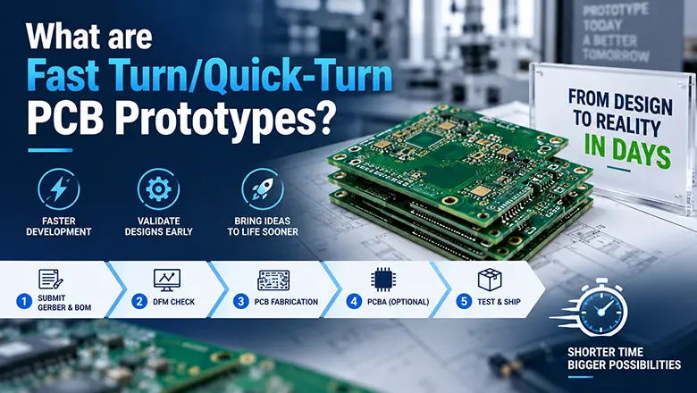
A fast turn prototype pcb (or quick-turn pcb prototype) is a low-quantity, rapid delivery printed circuit tailored for testing design concepts. Unlike regular production boards that may take weeks, these prototypes can be delivered in as little as 24 to 72 hours, depending on design complexity and pcb manufacturer capabilities.
- HDI and advanced technology boards: Current rapid prototyping services now offer capabilities such as HDI, blind and buried vias, impedance control, and fine-pitch BGA packaging—technical features that were previously typically limited to mass production but can now be realized at the prototype stage.
- From Prototype to Production: A robust rapid prototyping process not only supports early-stage design verification but also lays the foundation for subsequent mass production, facilitating a smooth transition from small-batch pilot runs to full-scale manufacturing.
When Are Fast Turn PCBs Used?
- First prototypes for new electronic products (consumer, automotive, industrial)
- Low-volume PCB runs for university or R&D projects
- Evaluating alternative layouts via custom prototype iterations
- Urgent respins due to late-stage design changes
How Fast Prototype PCB Services Work
The fast prototype pcb process is dynamic and collaborative, spanning from design submission to assembly and shipment.
Step-by-Step Quickturn PCB Prototyping Process
- Design Submission: Clients submit the complete design package—including Gerber files, BOMs, netlists, and assembly drawings—via our online quotation portal. When uploading, please ensure the layer stack-up definition is complete (covering copper, solder mask, and silkscreen layers) and clearly specify requirements such as impedance and special processing techniques to facilitate accurate production scheduling.
- DFM/Engineering Review: Upon receipt, our engineering team conducts a systematic DFM (Design for Manufacturability) review. We evaluate factors such as routing density, trace width and spacing, via types (particularly HDI blind and buried vias), thermal distribution, and layer count to ensure compatibility with our manufacturing capabilities.
- Rapid PCB Fabrication: Once the design is verified, your order is immediately placed in the priority production queue. Leveraging high-precision laser imaging, automated micro-via drilling and milling, and mature ENIG/HASL surface finishing processes, we rapidly manufacture rigid, flexible, or rigid-flex prototypes—ensuring excellent electrical performance and reliability—so you can receive the physical boards and begin testing without delay.
- PCB Assembly: Turnkey pcb assembly options—SMT and THT—enable fast, reliable population of pcbs with sourced or consigned parts. For prototypes, avoid hard-to-source parts that slow the entire production process.
- QA and Functional Testing: Visual inspection, electrical testing, and sometimes basic functional testing is included. This step verifies solder quality, circuit continuity, and eliminates early defects.
- Shipping and Logistics: Express shipment with tracking ensures boards arrive on schedule. Lead time for fast PCB prototype deliveries can be as short as one day for simple rigid pcbs using in-stock materials.
Selecting the Right Fast Prototype PCB Manufacturer/Partner
What to Look For in a Reliable PCB Manufacturer
- Specialization in Fast Prototyping: A truly agile service provider must reliably meet delivery schedule commitments while providing clear, traceable DFM (Design for Manufacturing) review records. Communication throughout the process should be direct and efficient, ensuring timely feedback on any issues.
- Advanced Technology: It is essential to verify the supplier’s mass-production capabilities regarding HDI, multi-layer lamination, Any-Layer Interconnect (ALIC) technology, and various via structures. They should also provide clear process parameter specifications—such as minimum trace width/spacing, via diameter tolerances, and aspect ratios.
- Product & Market Experience: Consider the supplier’s client base; a diverse portfolio covering startups, university research projects, and established OEMs is a positive indicator. Furthermore, certifications such as RoHS, ISO, and UL demonstrate that the company has robust systems in place for process control and environmental compliance.
- End-to-End Manufacturing Service: If a supplier offers both PCB fabrication and SMT assembly services, it significantly reduces communication overhead and eliminates intermediate steps, thereby naturally ensuring a more reliable overall delivery schedule.
Proactive Questions to Ask
- What’s your typical turnaround for 2-4, 6-8, or 12+ layer prototype PCBs?
- Are Gerber files and DFM feedback included in your prototyping package?
- Can you support my design complexity (hdi, rigid-flex, controlled impedance)?
- What steps do you take for quality pcb build and rapid turnaround?
PCB Design for Fast Prototype PCB Success
Design for Manufacturability and Testability
- Follow DFM guidelines: Use standard trace widths, spacing, and via sizes found in your manufacturer’s design tools or online calculators.
- Limit initial design complexity: Focus your first prototype on critical functions. Minimize advanced stackups, custom board size, or unique features.
- Verify all design files: Gerber file naming, consistent BOMs, and explicit assembly drawings are required for rapid prototyping and error-free fabrication.
- Address manufacturability for assembly: Ensure components are available, footprints standard, and pin 1/polarity clear on all devices.
Automate and Peer Review
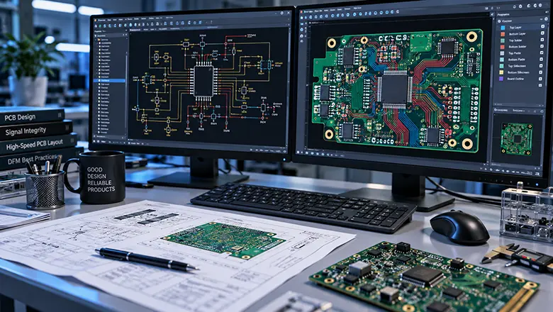
Mainstream EDA design tools (such as Altium Designer, KiCad, and OrCAD) now incorporate features like DFM analysis, error highlighting, and netlist verification. Designers are advised to fully utilize these automated checks before submitting files for fabrication, thereby catching most design-related issues prior to the manufacturing stage. For rapid prototyping projects, it is further recommended to create a self-check list to ensure all critical elements are thoroughly addressed.
- All copper, solder mask, and silkscreen layers are present in the Gerber file package.
- Vias and pads conform to your manufacturer’s manufacturing capabilities—especially for HDI designs or microvia layouts.
- Layer count matches your intended stackup for proper impedance control or multi-channel circuit complexity.
- Board edges, fiducials, and mechanical outlines are included for precise PCB fabrication and assembly.
PCB Materials, Stackups, and Technologies for Fast Prototyping
PCB Material Selection
The performance of rapid prototyping boards depends heavily on the choice of substrate material. Thanks to its mature supply chain, stable dielectric properties, and reasonable cost, FR-4 is the material of choice for the vast majority of prototyping projects. However, when designs involve RF applications, impedance control, or high-frequency signal transmission, specialized materials such as Rogers or polyimide may be required; as stock levels for these materials often fluctuate significantly, it is advisable to verify availability with suppliers before placing an order to avoid procurement delays affecting the overall delivery schedule.
- Common Quick-Turn PCB Stackups:
- 2–4 layer standard rigid PCB (fastest TAT, simple prototypes)
- 6–8 or 10+ layer PCBs for advanced technology boards (more design validation, HDI, microvias)
- Flex and rigid-flex printed circuit boards for wearables, IoT, or space-constrained prototypes
- Surface Finish Choices:
- HASL: Suitable for standard prototype boards, this option offers short lead times and low costs, making it an economical choice for the early functional verification stage.
- ENIG: It offers superior surface flatness and excellent oxidation resistance, making it particularly well-suited for high-density assembly involving fine-pitch leads and BGA packages. In terms of SMT yields and long-term reliability, it is often a worthwhile investment.
Vias and HDI Features
Modern rapid prototyping services now widely support blind, buried, and stacked via technologies—processes that are virtually indispensable for High-Density Interconnect (HDI) designs, high-pin-count components, and complex product structures. To ensure a smooth fabrication process, please clearly indicate these via types and their corresponding layer stack-up relationships when generating Gerber files and assembly drawings.
Best Practices for a Fast PCB Prototype Project
Streamline Your Design and Communication
- Limit initial prototype board complexity, focusing on core areas.
- Use panelization for multiple variants or parallel design exploration.
- Communicate design requirements, design files, and desired turnaround clearly and early.
- Confirm manufacturing standards or DFM notes from your PCB manufacturing partner.
Plan and Document Every Step
- Use file naming conventions and version control to prevent confusion over which Gerber file or BOM is current.
- Store approved stackups, layer count documentation, and reference PCB layouts for future prototyping rounds.
Leverage All Manufacturing Capabilities Offered
- Choose manufacturers with advanced technology (HDI, fast via drilling, controlled impedance) to future-proof your rapid prototyping pipeline.
- Ask about assembly capabilities: can they do turnkey PCB assembly, or will you need to handle component sourcing and placement yourself?
Fast Prototype PCB Project Best Practices
| Best Practice | Why It Matters for Rapid PCB Prototyping |
| Minimize initial design complexity | Faster fab and easier DFM feedback |
| Use standard materials and stackups | Lower cost, fastest board fabrication |
| Panelize variants for parallel testing | Accelerates learning and error detection |
| Confirm DFM and assembly drawings | Reduces avoidable manufacturing errors |
| Prioritize communication with supplier | Ensures on-time, accurate quick-turn pcb deliveries |
Common Fast Prototype PCB Challenges (and Solutions)
Design or Documentation Issues
- Incomplete or incorrect Gerber files:This is the primary cause of delays in PCB fabrication. It is recommended to perform a self-check using a Gerber viewer and run DRC and DFM analyses before submitting your files.
- Sourcing challenges: For initial prototype runs, try to avoid obscure components that have been discontinued.
- Layer count mismatch: Before placing an order, verify that your chosen supplier can accommodate your target layer stack-up within the promised lead time.
Supply Chain and Fabrication Delays
- Material shortages: During the design phase, prioritize the use of commonly available base materials and auxiliary components, and confirm sufficient current inventory with suppliers before finalizing the design.
- Assembly capacity bottlenecks: If the project involves SMT (Surface Mount Technology) assembly, it is advisable to schedule production line time concurrently, taking care to avoid industry peak seasons.
Functional Testing Gaps
- Design explicit test points and include a simple test protocol in your shipment for every prototype.
- For critical functions (RF, high-voltage, high-speed IO), specify functional testing options with your PCB manufacturer up front.
Testing and Quality Assurance in Fast Turn PCB Prototyping
Testing is your last line of defense against design errors or latent defects in quick-turn PCBs. Combine the following approaches:
- Visual inspection for solder bridges, HASL/ENIG finish quality, silkscreen/marking accuracy, and mechanical dimensions.
- Electrical testing (continuity, shorts, opens) as standard on all prototype boards from reputable suppliers.
- Functional testing: Power up the finished prototype, check regulator rails, clock oscillators, and any critical signal paths—ideally with a digital or automated test setup.
Quality Checks in Fast Prototype PCB Builds
| QA Step | Detects | Tool or Method |
| Visual Inspection | Solder, silkscreen, markings | AOI/manual lens |
| Electrical Testing | Shorts/opens on nets | Flying probe, bed of nails |
| Functional Testing | Real circuit performance | Bench test, firmware |
Pro Tips to Accelerate Your Fast PCB Prototype Turnaround
- Lock your design files early.The biggest delays come from mid-fab changes.
- Batch order boards for several design variants or teams and panelize where possible.
- Order extra boards and stencils—these pay for themselves by reducing the “rush to reorder” from initial failures or last-minute insights.
- Utilize turnkey PCB assembly for the quickest finished prototypes—fully sourced, populated, and tested by your manufacturing partner.
- Schedule daily standups with your team; immediate test feedback and a rolling “issues log” shaves days from total turnaround time.
Delivery and Shipping for Fast Prototype PCB
- Express courier (DHL, UPS, FedEx) is a must for international fast PCB projects; a day saved in transit can mean a week’s head start over competitors.
- Prepare import/customs paperwork.Mark your boards as “prototype pcbs” or “engineering samples” and avoid ambiguous product descriptions that get held up in customs.
- Track every shipment.Use your manufacturer’s portal and subscribe to real-time alerts for delivery status.
Cost Factors & Optimization in Fast Prototype PCB
- PCB complexity, layer count, and technology: More layers, HDI, or controlled impedance raise prices and may add lead time.
- Material selection: Standard FR-4 and HASL are fastest, while exotic substrates (Rogers, aluminum core, high Tg) cost more and may slow production.
- Assembly options: Turnkey PCB assembly costs more per board but saves labor and reduces the risk of assembly errors, making it valuable for time-sensitive projects.
- Batching and panelization: Paneling similar variants or project batches can lower per-board costs by sharing set-up, board fabrication, and assembly costs.
Cost Optimization Table
| Factor | Effect on Cost & Turnaround | Strategy |
| Layer count/HDI | Increases both | Use only as needed at first |
| Material (FR-4 vs special) | Exotic costs/delays | Confirm with supplier, substitute |
| Assembly/manual vs turnkey | Turnkey faster, pricer | Use for urgent prototypes |
| Quantity/panelization | More = lower per-piece | Combine teams/variants in orders |
Case Studies & Examples of Fast Prototype PCB Success
Example 1: IoT Startup
An IoT team needed three design changes in two weeks. Using a China quick-turn PCB manufacturer, they iterated on three grounded antenna layouts and power supply circuits via batch panelized prototypes. Early field testing on prototype PCBs led to a single, stable version ready for mass production in less than a month.
Example 2: Automotive Design
Automotive engineers built custom “daughter” boards for CAN/LIN bus translation. A rapid prototyping supplier delivered finished quickturn PCBs—including assembly—in four days, allowing the integration team to debug the entire car control system before a regulatory test deadline.
Example 3: University Research
A university lab designed an HDI board with microvias for advanced wireless sensors. Their rapid PCB prototyping partner, familiar with academic needs and tight schedules, provided design-to-delivery in under a week. The research group shared and open-sourced their prototype success, gaining international collaborators.
Common Pitfalls to Avoid in Fast PCB Prototyping
- Neglecting DFM feedback from your manufacturer—always review (not just acknowledge) suggested changes!
- Failing to lock your BOM. Always secure last-buys on nearing EOL components to avoid mid-prototype shortages.
- Overcomplicating the First Prototype.Overloading the first pcb prototype with advanced technology, unnecessary features, or unproven circuit blocks often leads to increased fabrication time, more errors, and extended debugging cycles. Instead, use a minimal core feature set, stable architecture, and proven interfaces. Add complexity as your prototype PCBs iterate and only when prior boards validate those design choices.
Why Choose LHDTECH (Or Your Preferred Partner) for Fast Prototype PCB
The right fast prototype pcb manufacturing partner is foundational for a successful project. LHDTECH and similar leading quick-turn PCB manufacturers stand out due to several competitive advantages:
- Manufacturing Standards & Capabilities: ISO, UL, RoHS, and IPC-certified, supporting a wide range of stackups, circuit densities, and HDI technologies—critical for both custom prototype runs and transition to mass production.
- Rapid Turnaround: Dedicated prototype PCB manufacturing lines, advanced PCB fabrication tools, and flexible scheduling enable 24–72 hour turns for urgent boards.
- End-to-End Service: From DFM-backed design review, Gerber file correction, and engineering support to reliable PCB fabrication, quick-turn assembly, and global logistics.
- BOM Optimization and Sourcing: Streamlined supply chain for in-stock parts, turn-key assembly with optional test services, and transparent communication at every stage.
- Post-Prototype Support: Smooth prototype to production scaling, quality control, and continued engineering collaboration even after initial delivery.
Emerging Trends and the Future of Rapid PCB Prototyping
Automation and Online Integration
- AI-Powered DFM & Design Tools: Expect smarter error-checking, automatic stackup guidance, and auto-generated assembly files—making prototype PCB success easier and faster.
- Fully Automated Quoting & Status: Major PCB manufacturers now offer instant quoting, project tracking, and live engineer chat integrations on their platforms.
- Prototype-to-Production Bridges: Increasing numbers of suppliers seamlessly convert a validated prototype PCB into a full production build, with zero lost context.
Technologies Driving Speed
- Universal support for HDI, blind/buried vias, microvias, and impedance-controlled stackups—even in fast PCB prototyping runs.
- Wider adoption of flex, rigid-flex, metal core, and ultra-high layer count boards in timeframes previously limited to standard rigid circuit boards.
Globalization & Customization
- More US/EU onshore fast-turn PCB suppliers are appearing, but overseas partners still set the pace for cost, range, and 24/7 service.
- Real-time logistics tracking, customs automation, and integrated component availability databases further boost rapid turnaround and supply chain stability.
Conclusion: How to Get a Fast PCB Prototype and Succeed in Rapid Development
Delivering a quality fast prototype PCB on time requires clear goals, the right supplier, and rigorous attention to the whole project lifecycle—from PCB design to functional testing and final global shipping.
Action Checklist
- Confirm design requirements and objectives.
- Create thorough, error-free design files—including all Gerber, BOM, and assembly drawings.
- Choose a responsive quick-turn PCB manufacturer, ask for DFM review.
- Use standard PCB materials and finishes (FR-4, HASL, ENIG) unless your design demands more.
- Schedule functional testing and quality checks for every iteration.
- Communicate design changes, lead time needs, and urgent issues promptly.
- Leverage advanced technology, real-time tools, and collaborative platforms for every phase.
- Use your prototype findings to improve manufacturability, documentation, and future product development cycles.
FAQs About Fast Prototype PCB
1. What is a PCB prototype?
A PCB prototype is an early version of a printed circuit board produced in small quantities to verify circuit design, functionality, manufacturability, and performance before mass production.
2. How fast can I get a PCB?
A fast prototype PCB can typically be manufactured in 24–72 hours for standard designs. More complex multilayer, HDI, impedance-controlled, or special-material PCBs may require additional production time.
3. How can I get fast PCB production?
Provide complete and manufacturing-ready Gerber files, drill files, stack-up requirements, board specifications, and special process notes. Clear documentation and standard materials can significantly reduce engineering review and production time.
4. How much does a 2-layer prototype PCB cost?
The cost of a 2-layer prototype PCB depends on board size, quantity, material, copper thickness, surface finish, minimum trace/space, and delivery time. Standard FR-4 prototypes are usually the most economical option.
5. What affects fast prototype PCB cost?
Key cost factors include layer count, PCB size, quantity, material, copper weight, surface finish, impedance control, via technology, testing requirements, and turnaround time. Faster delivery may also increase manufacturing costs.
6. Can I design my own PCB for prototyping?
Yes. PCB design software such as KiCad, Altium Designer, and Eagle can be used to create prototype PCB layouts. Before manufacturing, the design should pass DRC and DFM checks to reduce fabrication risks.
7. What PCB material is best for high-speed prototype designs?
FR-4 is suitable for many digital prototypes, while high-frequency materials such as Rogers laminates are preferred when low dielectric loss, stable impedance, or RF performance is required.
8. Why do prototype PCBs fail?
Prototype PCBs may fail because of design errors, incorrect footprints, poor routing, inadequate clearances, impedance issues, manufacturing defects, or assembly problems. DFM and electrical testing help identify these risks early.
9. Are prototype PCBs hard to manufacture?
Standard 1-layer and 2-layer prototype PCBs are relatively straightforward to manufacture. Complexity increases with multilayer stack-ups, HDI structures, blind/buried vias, fine-pitch components, heavy copper, or controlled impedance.
10. Which is better for testing, a PCB prototype or a breadboard?
Breadboards are useful for simple early-stage circuit testing, while PCB prototypes provide more accurate electrical, mechanical, thermal, and high-frequency performance. A prototype PCB is generally preferred before moving to production.