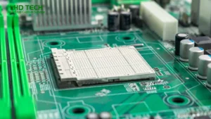
What is a Single Layer PCB?

One type of board that LHD TECH often makes is called single-sided PCB or a one layer PCB board, also known as Single layer PCB. It is the most basic type of printed circuit board with a very simple structure – just an insulating board (made of materials like FR-4, CM-1 or CM-3), with conductive copper foil laminated on only one side. All the electronic components are soldered on this side and connected by single conductive layer of copper foil.
This type of board is designed for products that do not require complex circuits, mainly featuring simplicity, fast delivery and low cost. In common items like LED lights, calculators, remote controls, and basic power supplies, this type of single-layer board is basically used.
If your product is also of this type, you’ve come to the right place. LHD TECH specializes in making this kind of board, which is reliable and worry-free.
The Simple Structure of Single Sided PCBs
The simple structure of a single-sided PCB is its biggest strength:
- Base Material (Substrate):It is the framework of the board, like FR-4 fiberglass board and CEM-1, which are hard and durable. Occasionally, flexible materials are also used, depending on the product requirements.
- Conductive Layer: One side is covered with copper foil, which is generally 1 to 3 ounces (per square foot) thick, and it is entirely dependent on it to run the circuits.
- Solder Mask (Insulating Ink): It is that layer of green oil on the board (there are also other colors) that covers most of the copper surface, only exposed at the pads, to prevent oxidation and avoid solder bonding during soldering.
- Silkscreen Layer: The characters and boxes printed on it indicate the positions, models and so on of the components. When we assemble and repair the board, we all rely on them for guidance.
Types of Printed Circuit Boards
Printed circuit boards are broadly classified by the number of conductive layers:
- Single Sided PCB: There is copper on only one side, and all the components are squeezed onto this side. It has the simplest structure and is suitable for products with uncomplicated functions.
- Double-Sided PCB: Both the upper and lower surfaces can be wired, and vias (through hole) can be drilled in the middle to connect them. This makes it much more flexible. Many regular electronic products use it.
- Multilayer PCBs:For instance, 4 layers, 6 layers or even more, it’s equivalent to pressing several layers of boards together and connecting them through vias in the middle. The lines can be laid very densely and the signals are cleaner, making it suitable for high-performance and highly integrated devices.
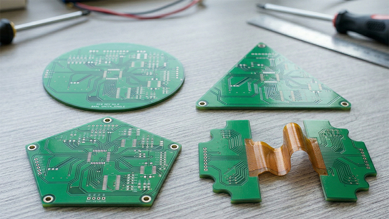
- Flexible and Rigid-Flex Boards:The board can be bent, making it suitable for structures that require folding or have limited space, such as flat cables and foldable screens. The rigid-flex board is a combination of a flexible board and a rigid board, which is both strong and flexible.
| Type of Printed Circuit Board | Copper Layers | Common Applications | Surface Mount? |
| Single Layer (1-layer) | 1 | LED, toys, remotes | Yes |
| Double-Sided | 2 | Power supplies, sensors | Yes |
| Multilayer | 4–60+ | Smartphones, routers, servers | Yes |
| Rigid-Flex | 2–10+ | Medical, aerospace, wearables | Yes |
Materials Used in Single Layer PCB Manufacture
PCB manufacturing begins and ends with materials selection—a crucial factor affecting electrical performance and cost.
- FR-4:This is the most common board material, glass fiber combined with epoxy resin, which has good strength and does not absorb water. The vast majority of standard products use it, which is safe and reliable.
- CEM-1 and CEM-3: These two models offer better value for money. One is based on paper and the other is made of fiberglass composite. They are more than sufficient for ordinary appliances with low requirements and can save costs.
- Flexible Substrates: This type is specifically designed for flexible circuit boards. It can be bent and folded. Smart wearables or places where wiring is needed all rely on it.
- Aluminum Core: There is a layer of aluminium at the bottom of the board, which conducts heat particularly well. For our high-power LED lights and power boards, it is essential to use it as it has fast heat dissipation and is durable.
Unique Advantages of Single Layer PCBs
Single layer PCBs offer unique advantages when compared to more complex multi-layer boards:
- Cost Efficient:It uses less materials, has a simple production process and a smooth flow, making it particularly suitable for mass production and helping you save on budget.
- Simple Structure: It’s just one layer. The design is not brain-taxing and is particularly suitable for beginners to practice or for quick prototyping.
- Quick Manufacturing Turnaround: For sample production, it can be done within a few hours, and the batch production is also very fast, which won’t delay your project rush.
- Ease of Assembly and Repair: All components and circuits are fully exposed, making soldering, inspection and repair very convenient. It’s easy to tell at a glance where the problem lies.
- Thermal Management: With the right substrate, even single-sided boards can offer good heat conduction (aluminum substrates) for PCB applications like LED modules.
- Ideal for Wide Range of Applications: From remote controls, vending machine circuits, and toys to basic household appliances, their flexibility is unparalleled.
Limitations Compared to Multilayer PCBs
While single-sided boards are champions of affordability and speed, they do have notable limitations:
| Limitation | Impact on Design/Use |
| Trace Routing Limits | Cannot support high-density or complex circuitry |
| Signal Transmission | Susceptible to crosstalk and EMI due to proximity of traces |
| No Ground Plane | Harder to manage electrical performance in sensitive circuits |
| Board Size | Larger sizes needed for more components |
| No Advanced Features | Lacks features enabled by multiple layers such as impedance control, power/ground planes |
A Guide to Design: Step by Step

Let’s detail a practical guide to design a single layer PCB with top electrical performance and manufacturability:
- Define Circuit Requirements: Clarity at this stage prevents costly reruns in production.
- Schematic Capture: Draw your functional circuit, considering single-sided routing.
- Component Placement: Arrange all electronic components on one side. Place high-priority items first for optimum signal flow and heat management.
- Trace Layout: If the line can go straight, don’t take a detour, especially avoid crossing. Only in this way can the signal be stable.
- Decoupling Capacitors: The decoupling capacitor should be as close to the IC as possible, which can effectively suppress noise and voltage fluctuations.
- Thermal Considerations: If the power of the board is high (such as LED lights or power supplies), don’t hesitate to directly apply an aluminum substrate. Fast heat dissipation leads to a long lifespan.
- Design Rules and DFM (Design for Manufacturability): The production capabilities of line width, line spacing and hole diameter vary from manufacturer to manufacturer. Communicating in advance can save the trouble of going back and forth to revise the manuscript.
- Generate Gerber Files and BOM: The Gerber files (layers such as copper foil, green oil, and silk-screen printing) and the BOM list (component list) must all be prepared, whether for sample making or batch production. This is a standard configuration.
- Prototype and Test: First, make a small batch, solder the components and actually test them – power on to see if the performance and signal are correct, and then stuff them into the casing to test the size. It’s the safest to increase production only when there are no problems.
Key Considerations for Superior Circuit Board Design
Best practices and tips for robust, low-cost, high-quality single-sided PCBs:
- Optimize Circuit Pattern: Group related signals and components together. Maintain short, direct paths between connectors and major ICs.
- Trace Width and Thickness: Use software or online calculators to set trace width/copper weight for expected current. For example, 1 ounce per square foot copper is common for signal traces, but power traces on motor controls may need 2–3 oz.
- Place Test Pads:Leave several points on the board where the probe can be inserted and mark them clearly. It will be much more convenient for quality standards or on-site maintenance later.
- Avoid Sharp Corners: If possible, round the corners. Not only is it easier to produce, but the copper sheet is also less likely to crack and more durable.
- Strategic Use of Ground Fills:The exposed areas of the board should be covered with copper sheets for grounding as much as possible. Although there is no dedicated ground layer, it can play a shielding role and suppress electromagnetic interference.
- Consider Flexible Substrates for Challenging Geometries: If the shell structure is special and requires bending, choose flexible substrates such as polyimide or PET. Soft boards can also be made into single-sided boards, and the problem can still be solved.
The Manufacturing Process of Single Layer PCBs
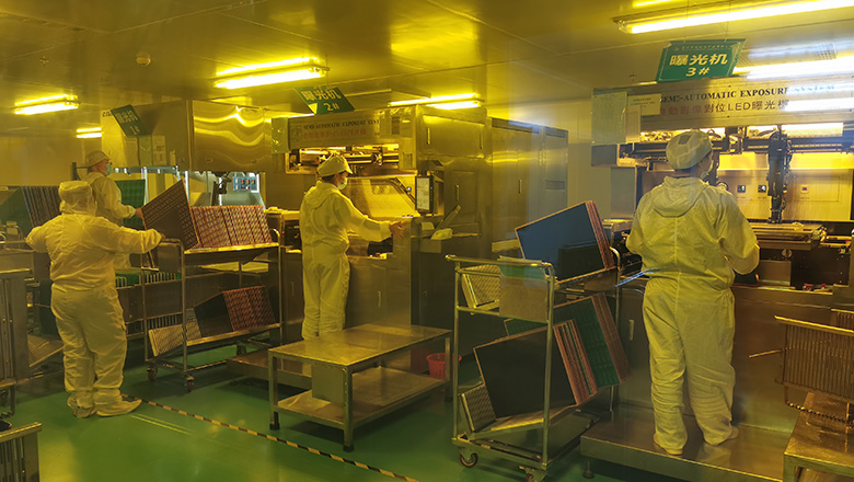
Modern PCB manufacturing combines precision, speed, and affordability for single-sided designs. Here’s an overview:
- Substrate Preparation: Prepare a large sheet of substrate material (FR-4, CEM-1 or aluminum substrate), and with a thin layer of copper foil on one side first.
- Image Transfer: Print the circuit pattern onto the copper surface by photosensitive method, and protect the areas that should be left.
- Etching: Use chemical solutions to etch away the unprotected copper, and what remains is the circuit.
- Drilling: Drill out the component holes of the plug-in. Single-sided panels do not require vias, which is a very fast step.
- Solder Mask and Silkscreen: Apply a layer of insulating ink (or other color) to cover the copper wire, leaving only the pad position exposed, and then print the component symbols.
- Surface Finish:The pads should be coated with surface coatings, such as tin spraying (HASL), gold plating (ENIG), or OSP, to facilitate soldering.
- Panelization and Cutting:Small panels are assembled into large ones for production together, and then separated by V-cut or milling, which is highly efficient.
- Inspection and Testing: At each process, there is visual inspection or AOI (Automatic Optical Inspection) monitoring. Finally, power is applied for testing to ensure that the board is in good condition before shipment.
Key Production Steps and Stakeholder Benefits
| Step | Purpose | User Benefit |
| Image Transfer | Transfers accurate layout | Ensures design-to-board fidelity |
| Etching | Removes excess copper | Reliable signal routing |
| Solder Mask | Prevents shorts, protects copper | Durability, longer life |
| Surface Finish | Prepares pads for soldering | Easier assembly, better quality |
| Testing | Electric and visual quality check | Fewer field failures, high yield |
Assembly and Prototyping: From PCB Board to PCBA
The production of the board is just the first step. The next step is to install the components – from a plain board to a functional PCBA (Printed Circuit Board assembly). Leave this step to LHD THC, and you can rest assured.
- Component Placement: All components are placed on the side of the single-sided panel that is attached to the components. Whether it is through-hole or surface mount technology (SMT), they are all within the scope of our production processes.
- Soldering: For through-hole components, wave soldering is generally used, while for surface mount components, reflow soldering is chosen. After the processing operation by the machine, the solder joints are completely stable.
- Prototype Assembly: When the quantity is small or there are only a few samples, our professional engineers manually attach and weld them, and then check each one to ensure there are no issues.
- Mass Production Assembly: When the volume is large, it becomes fully automated. The entire process, including machine surface mount technology (SMT), assembly line welding, and automatic optical inspection (AOI), is fast and efficient, ensuring that each board is consistent.
Testing and Quality Standards in PCB Manufacturing
In the product standards of LHD TECH, the quality control especially for bulk orders, which must be inspected layer by layer:
- Visual Inspection: First, go through it once to see if there are any minor issues such as solder connection, broken wires, or missing parts.
- Automated Optical Inspection (AOI): The machine automatically scans. Whether the solder joints are straight or not and whether the components are pasted crooked can be identified at a glance by the computer.
- In-circuit Testing: Use a test stand or a flying probe to check if the circuit is working and if the voltage is correct. Only after testing can you feel at ease.
- Functional Testing: Simulate the actual power-on and run it. Whether the board can work normally is determined by this step.
Quality Standards to demand from your PCB manufacturer:
- IPC-A-600: The board itself must meet the standards.
- IPC-A-610: Components must also be qualified after soldering.
- RoHS Compliance:Materials must be environmentally friendly and contain no harmful substances at all.
Every board produced by LHD THC follows this process, and what you get is a high-quality PCB.
Choosing the Right Single Layer PCB Manufacturer
With thousands of global suppliers, how do you select the best single layer PCB manufacturer for your needs?
Checklist:
- Specializing in single-layer boards: We don’t aim for quantity. We just focus on making single-layer boards perfect and down-to-earth. We are not the kind of person who does everything but excels in nothing.
- Experience matches: We have made boards of any material, thickness or weight of copper sheet you need, and we have ready-made cases.
- We accept both large and small orders: samples for a few hundred yuan, mass production for tens of thousands of pieces. Our production lines can be flexibly switched, accompanying you from R&D to bestsellers.
- Complete certificates: International standards such as IPC, RoHS and ISO are all up to par, and there is no problem exporting globally.
- Accurate delivery time and prompt after-sales service: Once the delivery date is agreed upon, there will be no delay. If there are any problems, you can find someone, they will respond quickly and solve them decisively.
- The quotations are transparent and not concealed: how much it costs and how it is calculated are directly provided to you, and the speed is very fast.
Trends & Future Prospects in PCB Technology
Even as multilayer boards climb in use for smartphones and advanced electronics, the single-sided PCB is evolving:
- Eco-Friendly Materials: Nowadays, lead-free processes and green substrates are being promoted. Our production line has been running smoothly for a long time, making it more environmentally friendly.
- Finer Features, Better Performance: Although it is still a single-sided board, the current etching and photosensitive technologies can make the circuits both dense and precise, and even handle more complex designs.
- Automated Manufacturing & Smart QA: The production line is equipped with intelligent devices and AI optical inspection, ensuring a stable yield rate and no need to worry about quality.
FAQs: Expert Insights on Single Layer PCBs
Q: Can a single layer PCB be used in high-frequency circuits?
A: It can also run. The mid-frequency band is fine. Just use some good boards and pay attention to the wiring. But when it comes to true high frequencies and RF, multi-layer boards are still needed as they offer better control.
Q: How does a single layer PCB compare to a double-sided or multilayer PCB in terms of electrical performance?
A: After all, it doesn’t have a complete ground plane or vias, and its anti-interference ability for high-speed signals can’t keep up. For high-density and high-speed tasks, double-sided boards or multi-layer boards are still the best choice.
Q: Can I get flexible single PCB prototypes?
A: Sure! Our LHD TECH polyimide and other flexible materials are also frequently produced. Samples for wearable devices and irregular structures need to be made as quickly as possible.
Q: What determines the final cost of a single layer PCB?
A: Check the material, copper thickness, board size, complexity of the circuit, and surface treatment process. These items have been settled, and the price is almost certain.
Conclusion: The Future of Single-Sided Boards
Although multilayer PCBs and high-density interconnect boards are becoming increasingly popular nowadays, our LHD TECH single layer PCB remain an indispensable main force in the global electronics industry. What are you after? Just because its production process is smooth, the cost is kept low and the design is still practical. From small household appliances and daily equipment to professional lighting, basic power supplies, and even rapid prototyping, single sided PCBs can handle everything and still bear the pcb applications.
In summary:
- The single-layer board, to put it simply, is simple, reliable and low-cost. This is the mature board of LHD TECH.
- As long as the product does not have so many complex requirements, such as no need for multiple layers of wiring or dedicated layers, single-sided panels are the most suitable choice – they have a simple structure, fast delivery, and are easy to produce in large quantities.
- From sampling a few hundred pieces to mass production of several million pieces, LHD TECH can switch easily. The design basically doesn’t need major changes, which is worry-free.
- Despite the basic nature of single-sided panels, the current level of automation, material quality, and environmental protection processes have all caught up, and they can still meet the modern product’s requirements for quality and greenness.
When To Choose Single Layer PCBs
- You need a low-cost PCB board.
- The circuit is straightforward without requiring advanced signal transmission or EMI shielding.
- Easy repair, maintenance, and quick prototyping are priorities.
- The product is used in a high-volume, cost-sensitive market—like consumer remote controls, LED lights, or educational kits.
Best Practices Checklist
Before moving to production, verify the following:
- Your schematic and pcb design accommodates all needed electronic components on a single conductive layer.
- Selected substrate (FR-4, CEM-1 and CEM-3, aluminum core, or flexible material) meets mechanical, thermal, and budgetary requirements.
- Gerber, drill, and assembly files are error-free and DFM-verified.
- Decoupling capacitors are correctly placed for smooth electrical performance.
- Trusted PCB manufacturer with experience in single-sided and single layer PCBs is chosen.