
Introduction: The Importance of PCB Manufacture
The PCB manufacturing process serves as the fundamental support for every electronic innovation. The circuit operation of electronic devices such as mobile phones, laptops, automobiles, medical equipment and satellites all relies on printed circuit boards. Designers creating initial prototypes and engineers managing global PCB production both require an understanding of every step in the PCB manufacturing process.
This article analyzes the complete manufacturing process of printed circuit boards, which includes stages such as design, fabrication, drilling, plating and testing, concluding with the finished circuit board. These stages cover the best practices in manufacturing, with different types of circuit boards requiring different manufacturing approaches. This article explains how to ensure accuracy at every step from the schematic diagram to the final stage of production.
Understanding PCB and Circuit Basics
Printed circuit boards serve as both the skeleton and nervous system of modern electronic devices. As the skeleton, they establish the fundamental configuration of the circuit board and support the overall structure. As the nervous system, they map out the layout of circuit traces to ensure signal transmission. Printed circuit boards provide stable mounting support for electronic components, guaranteeing their reliable operation.
- PCB stands for: Printed Circuit Board.
- PCB comprises a laminate board made from fiberglass (FR4) or other materials.
- Copper foils in the printed circuit board form conductive circuits.Non-conductive layers provide mechanical support and electrical insulation.
Parts of the PCB
| Part of the PCB | Function |
| Copper Layer | Conducts electricity between components. |
| Substrate/Laminate | Support structure, typically made of FR4 or polyimide. |
| Solder Mask | Protects the copper layer, defines where solder sticks. |
| Silkscreen Layer | Adds markings, component values, and orientation. |
| Drill Holes | Allow placement of through-hole components and vias. |
The production process involves a sequence of manufacturing steps that take your design from idea to a physical PCB board. The circuit board fabrication process is closely tied to both the pcb design process itself and the specific needs of your product.
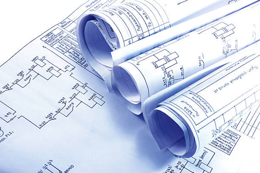
Starting Point: LHD TECH’S PCB Design Process
The journey begins long before fabrication—the first step in the PCB process is always pcb design and defining the pcb schematic.
Our PCB Design Steps
- Schematic Capture:Designers rely on PCB design software to carry out their work. Such software includes Altium Designer, KiCad, Eagle, OrCAD and others. The core function of the software is to construct the network of connections for electronic components.
- PCB Layout:Circuit designers convert circuit schematics into physical designs. They perform component placement on the circuit board in accordance with electrical and manufacturing standards, and carry out circuit routing in compliance with relevant professional specifications.
- Layer Definition:The designer decides if a single-layer, two-layer pcb or a multi-layer pcb best fits the application.
- Board Outline & Stack-Up:Define the size, edge cuts and the stack of layers of the PCB.
- Gerber & Drill File Generation:Convert your design into manufacturing files. The pcb design is approved once these files pass design and DFM review.
LHD TECH’S Step by Step Guide to the PCB Manufacturing Process
The pcb manufacturing process is a highly-regulated, precision-driven series of events. Let’s explore each major step of the printed circuit board fabrication process.
Step 1: The Design in a Process
Every pcb manufacture project starts with a circuit board design. Here, the designer chooses the layer count, sets up the pcb schematic, and creates the pcb layout with careful attention to clearances, drill holes and trace widths.
Key Actions:
- Define the stack-up for the new PCB.
- Place all required components and create a netlist.
- Export Gerber files and a drill data file.
Remember: The starting point for the PCB is always a solid, manufacturable design.
Step 2: From Digital Design to Photo Negative of the PCB
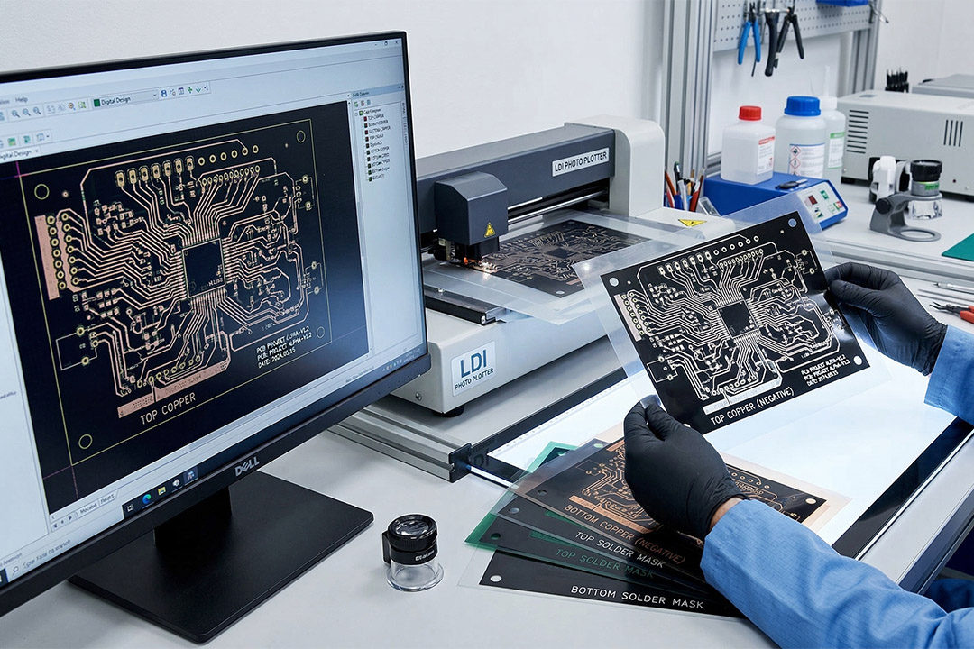
Subsequent processes in the PCB production flow complete the conversion of digital files into physical carriers. This physical carrier is a phototool specially designed for PCBs. The PCB phototool functions as a mask in the subsequent production steps.
Process Steps:
- Photo plotting:Films are generated for every copper layer and mask layer.
- Each two-layer PCB needs four sheets: top copper, bottom copper, top solder mask and bottom solder mask.
Why this step is critical: It helps define where exposed copper should remain on the board and guides the rest of the fabrication process.
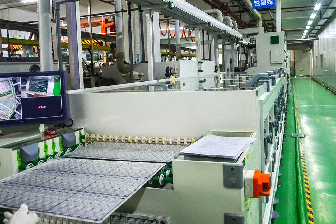
Step 3: Inner Layer Imaging and Etching Process
In multi-layer PCB fabrication, the process starts with the inner layers of the PCB.
- Opening Photoresist:Photoresist is laminated onto the core.
- Imaging:The photo negative is projected or printed onto the resist.
- Etching process removesthe exposed copper, so only copper traces on the layers (the required pattern) are left.
Key Terms and Insights:
- The etching process removes all the copper outside the desired circuit. This chemical process is often monitored to ensure precision.
- The actual PCB now takes shape.
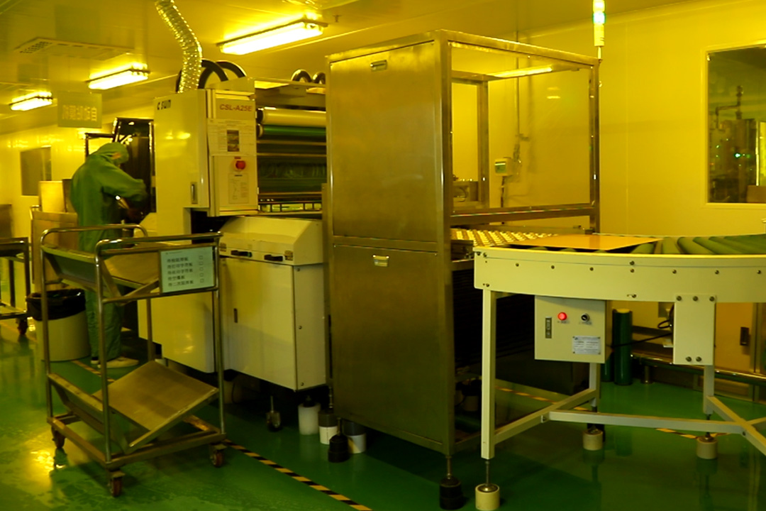
Step 4: Lamination Process — Layering the PCB Together
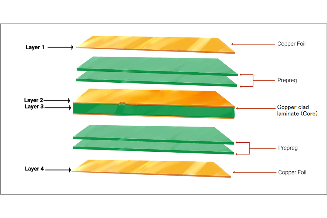
The lamination process carries out pressing operations on various independent plates.Etched cores, prepreg insulation layers and outer copper foils serve as the core components for lamination.The lamination process forms the final finished printed circuit board through tight bonding.
How the Process Happens:
- Stack-up:The preceding process completes the fabrication of each circuit layer of the circuit board.Operators finish the stacking and placement of the circuit layers in accordance with established design specifications.
- Prepreg (pre-impregnated resin):Used as an adhesive between layers of the PCB.
- Lamination press:The press applies heat and pressure to the entire laminated structure.High temperature and pressure fully melt the internal resin material.Molten resin firmly bonds all layers of the circuit board together.This process is a key step in printed circuit board manufacturing.
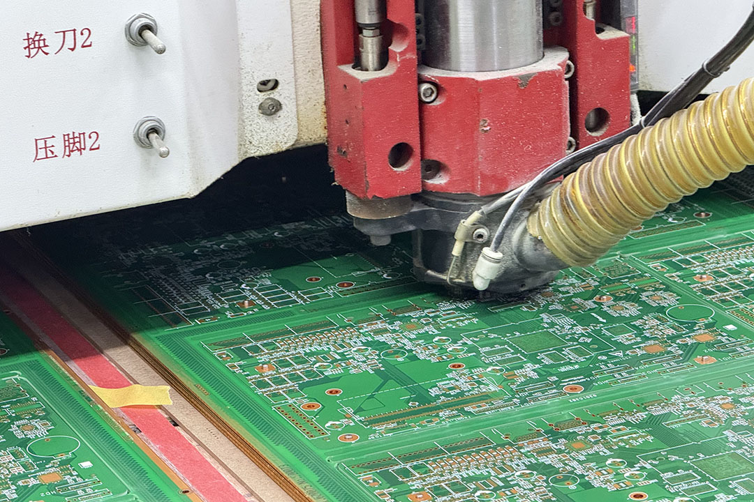
Step 5: Drilling the PCB
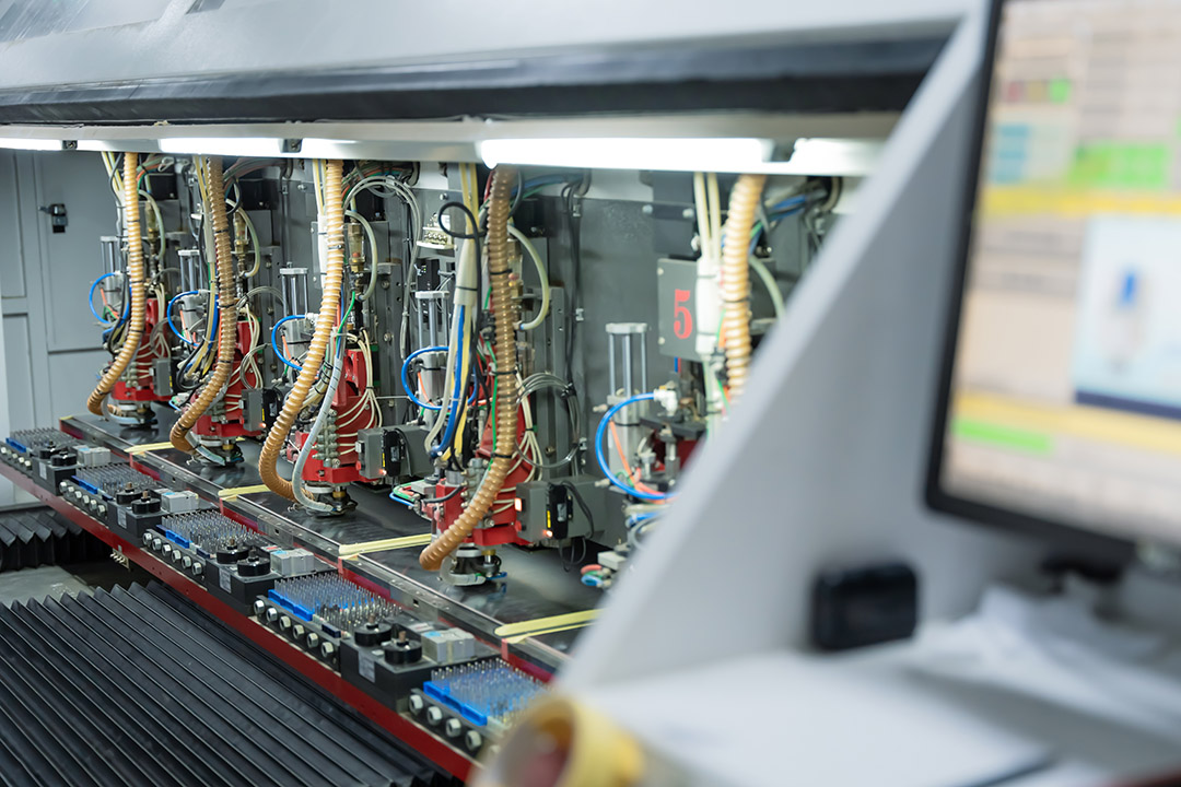
Drilling is central in both single, double and multi-layer PCB manufacture. Drill holes allow electrical connections (vias) and mechanical mounting.
- CNC Drilling Machine:Precision heads drill thousands of holes into the finished laminate stack.
- Blind/Buried Vias:Advanced boards use blind (surface to inner layer) and buried (between inner layers) vias, drilled into the PCB panel before or after lamination, depending on type. This step in the PCB manufacturing process demands high-accuracy equipment and process monitoring.
Essential Drilling Details:
- Drilling machine uses carbide or diamond-coated bits for standard and microvias.
- Drill holes are carefully positioned—too close to traces or copper edges risks short circuits.
Process requires: careful bit selection, controlled rotation speed, precise positioning.
Step 6: Plating Process & Chemical Deposition Process
After drilling, the fabrication process moves to the plating process, which gives electrical connectivity between layers.
How the Process Works:
- Chemical deposition process:The PCB undergoes cleaning, then is dipped in a series of baths depositing a thin (typically 1–2 microns) seed layer of copper throughout all drilled holes—a critical step forming plated-through holes and vias.
- Electroplating thickens copper on traces and inside holes, ensuring conductivity.
- Process involves:strict control of time, temperature and chemical concentration for high-quality results.
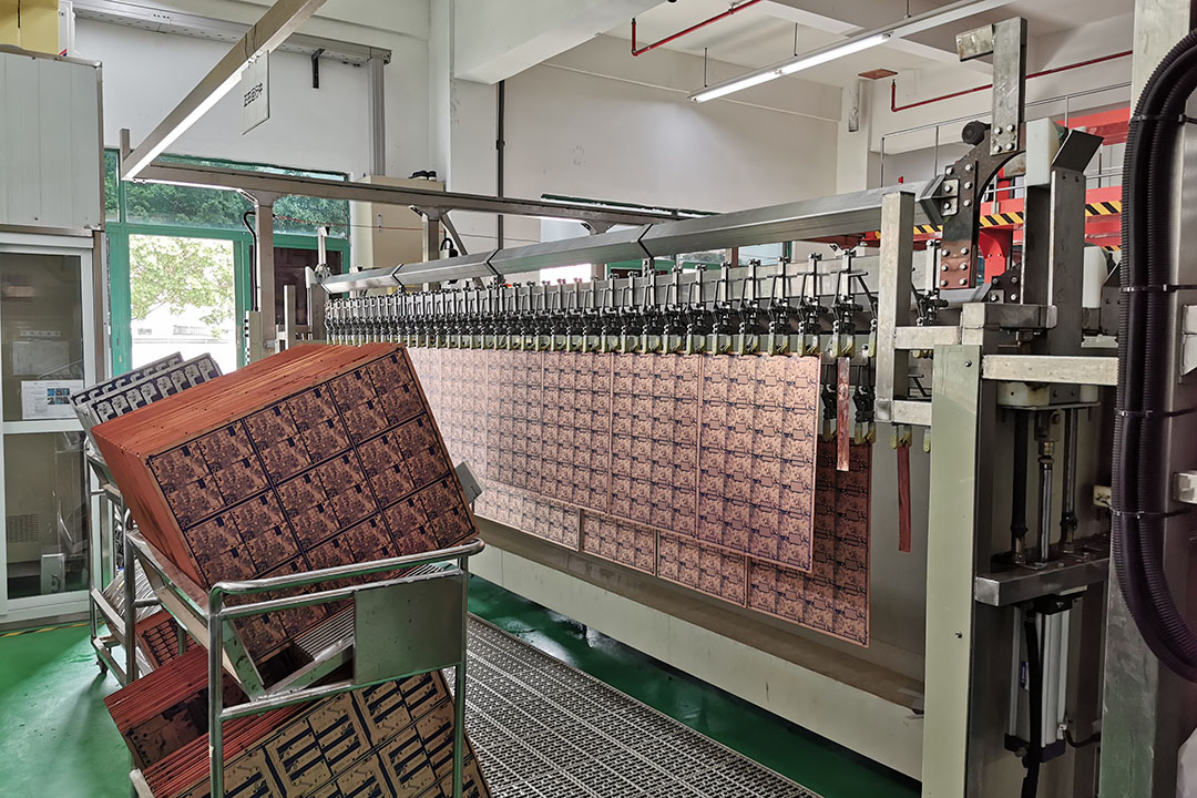
Step 7: Outer Layers and Etching Process Removes Unwanted Copper
Now, the outer layers of the PCB get their copper patterns.
Process Steps:
- Photoresist is again applied and imaged using the outer layer photo negative.
- Exposed copper areas are protected with tin or another etch-resist material.
- Etching process removes the unwanted copper, leaving intact the pads, traces and the necessary copper parts of the PCB.
Process removes: All copper not masked by the resist/tin, resulting in the final circuit pattern for component pads, signals and power delivery on the pcb surface.
Step 8: Solder Mask and Silk Screen
The distinctive green or colored coating you see on most PCBs is the solder mask layer. It’s crucial for assembly reliability.
Steps of PCB Solder Mask Application:
- Solder mask is applied and cured, leaving contacts and certain areas exposed copper for soldering.
- A silkscreen layer (white or contrasting color) is printed on top, providing part identification, values, and orientation.
- Layer of the PCB: Solder mask keeps circuits from shorting and secures solder only where required.
Step 9: Surface Finishes for the PCB Surface
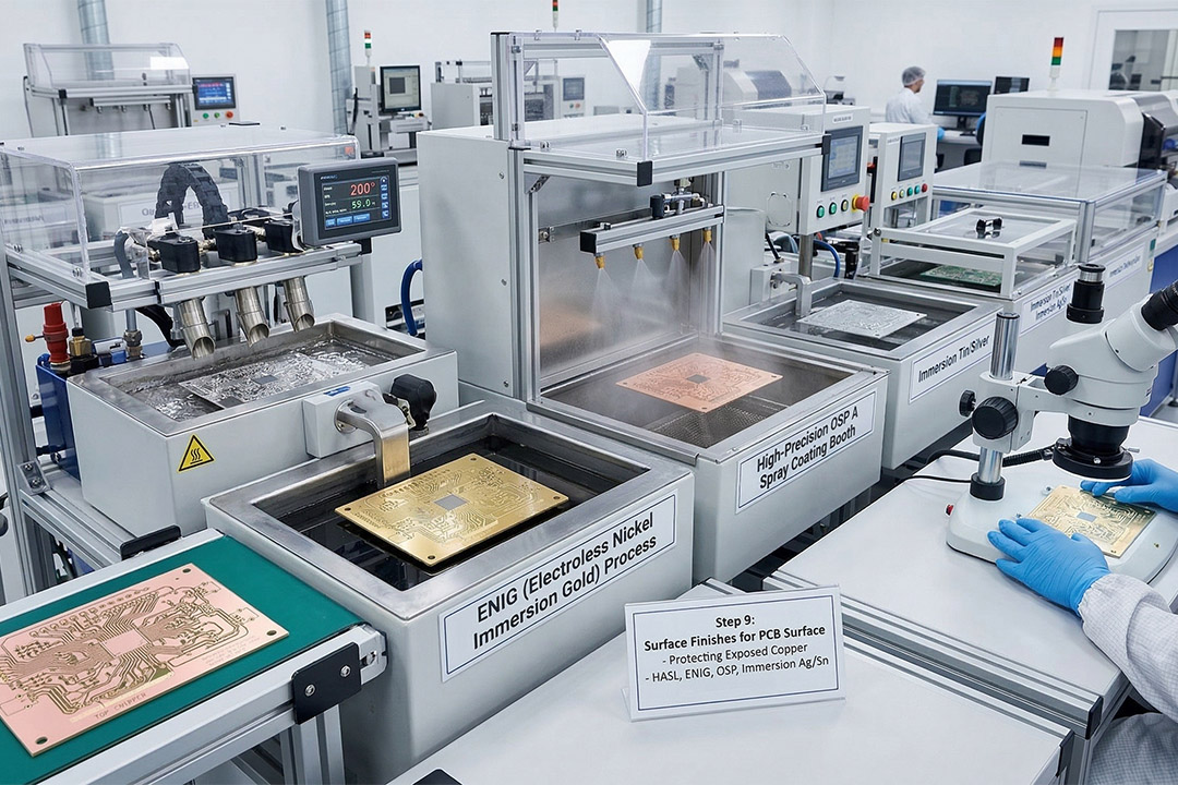
With the major pcb fabrication process steps finished, the exposed copper is vulnerable to oxidation. The pcb surface is protected and prepared for assembly by applying a surface finish.
Common Surface Finishes:
- HASL (Hot Air Solder Leveling)
- ENIG (Electroless Nickel Immersion Gold)
- OSP (Organic Solderability Preservative)
- Immersion Tin/Silver
Why it matters: The finish affects solderability, shelf life and electrical properties of the circuit board fabrication process.
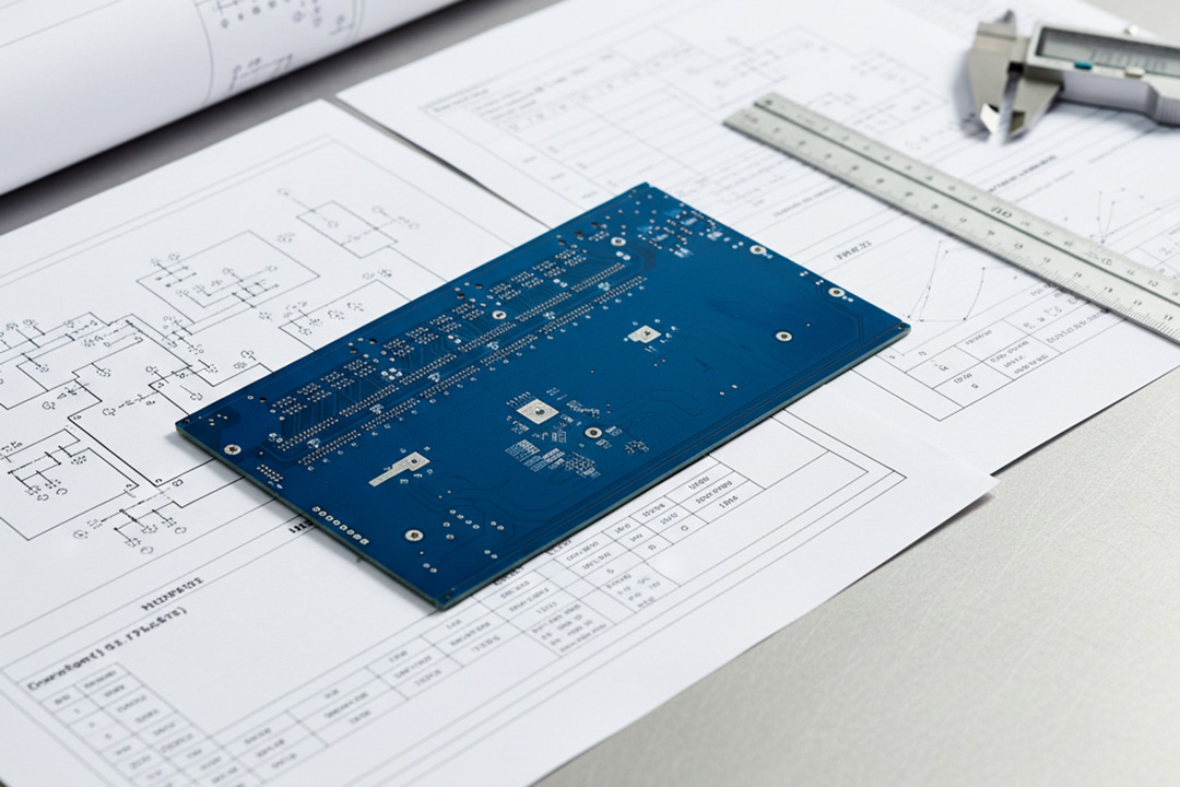
Step 10: Electrical Tests on the PCB and Final QA
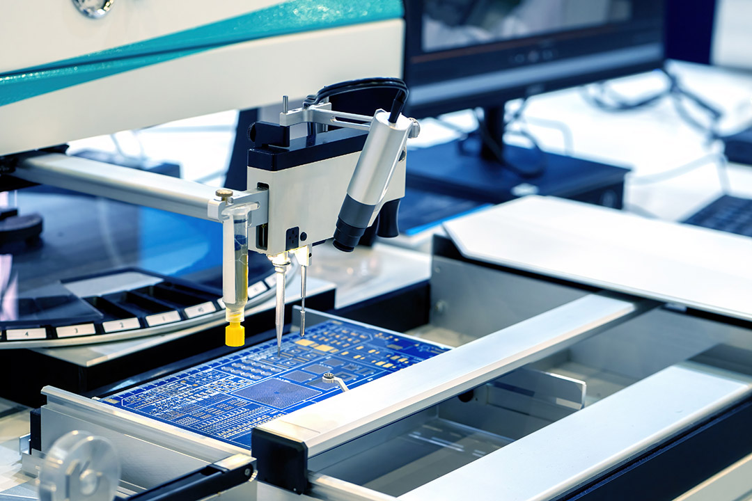
No professional PCB manufacturing process is complete without rigorous testing.
Testing and Inspection Steps:
- Electrical tests on the PCB: Continuity (are all intended connections present?) and isolation (are there shorts between nets?).
- Flying probe testing or bed-of-nails testing—technology choice depends on production volume and complexity.
- Visual/AOI (Automated Optical Inspection) checks pad sizes, silkscreen accuracy and finds solder mask errors.
The results ensure each finished PCB meets quality, reliability and safety standards before shipment.
Step 11: Routing, Profiling and the Last Step
The last step in the pcb manufacturing process is cutting the individual boards from the full pcb panel, also called depanelization.
How the Process Happens:
- V-scoring or routing: Boards are separated using a scoring blade or precision router. Small “tabs” support the PCB units until snapped apart.
- This step of the printed circuit and the entire production process guarantees individual boards are the right size and shape.
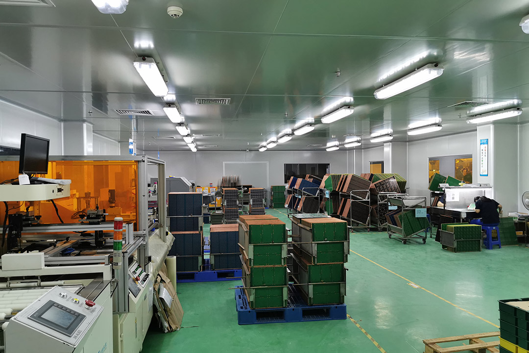
Step 12: PCB Packaging
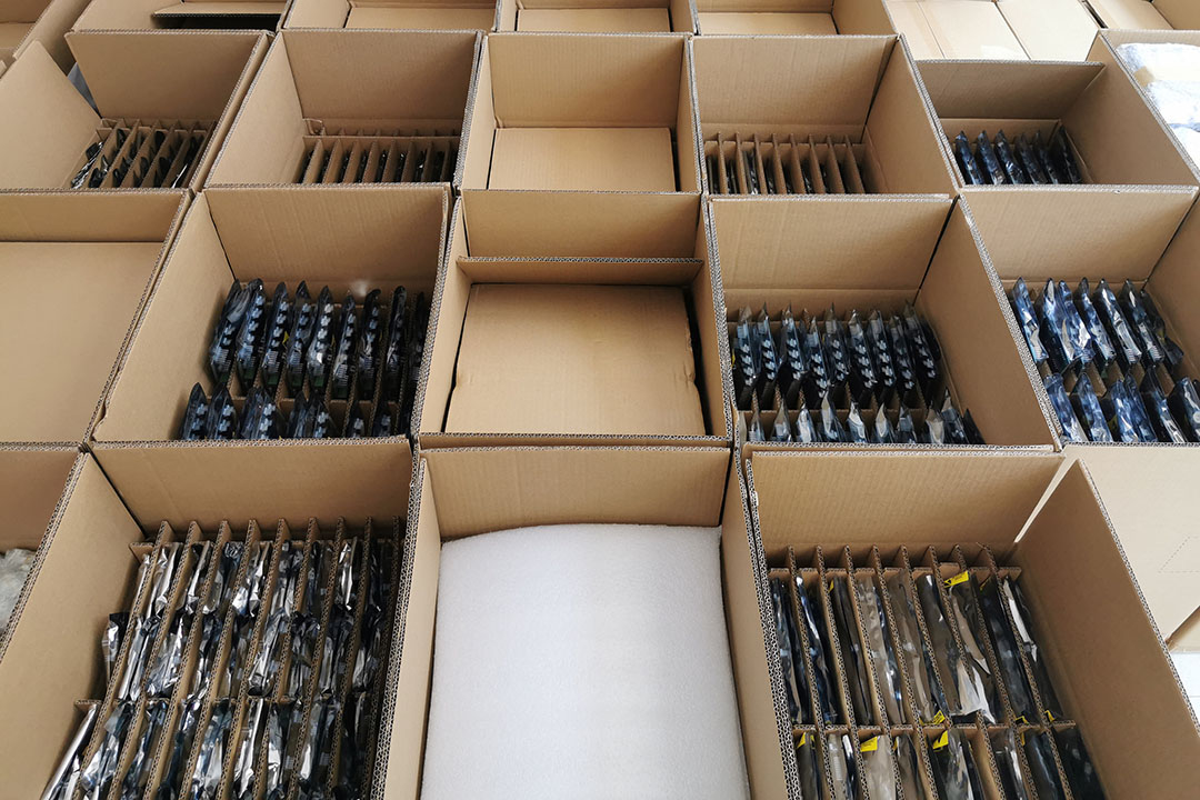
We understand that printed circuit lines are fragile and static electricity can pose a hazard, so we use the following packaging methods:
- Antistatic bag
- Shockproof bubble wrap
- Rigid reinforced cardboard box
Specialized & Professional PCB Manufacturing
Two-Layer PCB vs Multi-layer PCB
- Two-layer PCB:Simpler, uses top and bottom copper for signal routing. They need four sheets for film imaging and offer a balance between cost and complexity.
- Multi-layer PCB:Adds signal, power, and ground planes, crucial for modern, high-speed, low-noise designs. More manufacturing steps (extra imaging, lamination, drilling, layer registration) are required.
Layer Comparison
| PCB Type | Standard Layers | Typical Application | Process Complexity |
| Basic Form of PCB | 1 | Simple, low-power devices | Simple |
| Two-layer PCB | 2 | Most consumer, industrial | Moderate |
| Multi-layer PCB | 4–32+ | Aerospace, computing, RF | Advanced |
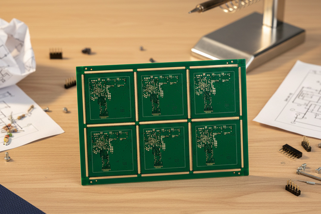
PCB Panelization, Units and Production Scale
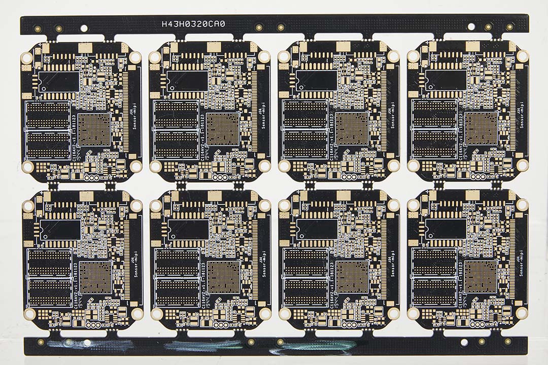
Large-scale pcb production is rarely about making a single board. Instead, boards are manufactured in arrays or panels, optimizing space and handling throughout the production process.
- PCB panel design helps reduce waste, speeds up assembly, and is essential for surface mount (SMT) lines.
- Separation (depanelization) only takes place after all steps of pcb manufacture are complete.
Panelization tips: Always coordinate fiducial placement, breakaway tab design, and stacking considerations with your manufacturer for maximum efficiency.
LHD TECH’S Advanced Tips for PCB Designers
- Select the right PCB manufacture process for your circuit’s needs:Consider cost, signal integrity, power capacity and environmental conditions.
- Include mechanical and manufacturing constraints in your PCB layout and design.
- Always consider the next step in the PCB process:Visualize how each previous step influences assembly and testing.
- Design for Test:Include test points in the PCB design process for every net required in functional QA.
- Communicate stack-up and finish needs:Outline whether your board needs special surface finishes or impedance control.
- Balance copper for warping prevention:The process of transferring the design to copper must keep copper balanced across layers for multi-layer PCB boards.
Conclusion: The Global PCB Fabrication Process in Summary
The PCB manufacturing process achieves effective connection between innovative electronic circuit concepts and tangible, reliable products.Various processes in PCB production cover the initial stage of schematic design, circuit routing, quality inspection and finished product delivery.The execution of all processes demands precise operation standards, strict control specifications and suitable professional technical conditions.
Professional PCB manufacturing processes have complete production capabilities.They can produce quick-turn prototypes and complex high-density multilayer circuit boards.The stability of product quality relies on multiple guarantee conditions.Advanced production equipment provides core hardware support.Early-stage design planning, communication and coordination, and inspections at each process jointly ensure product quality.
Whether you’re working with LHD PCB or a global PCB manufacturer, understanding every detail of the process and establishing partnerships with your right suppliers early on will ensure your next electronics project not only meets expectations but exceeds them.