Introduction to PCB OSP Surface Finish
In PCB manufacturing, protecting the exposed copper surface is crucial as it directly affects assembly yield, product reliability, and cost control. Organic solderability protectant (OSP), as a transparent, economical, and efficient surface treatment solution, is suitable for copper pads on rigid and flexible circuit boards and can effectively provide protection.
With the popularization of high-density mounting and lead-free environmental requirements, OSP surface treatment film has become one of the mainstream choices in the current circuit board industry. This process can prevent copper surface oxidation and maintain good weldability, which is the key to obtaining stable and high-quality solder joints
I would like to share some key points about what makes OSP the top choice for many PCB manufacturers, how this process works, the advantages and disadvantages of this process, and the key storage and processing techniques for maintaining the optimal state of OSP coating on circuit boards.
What is a PCB Surface Finish and Why is Surface Treatment Crucial?
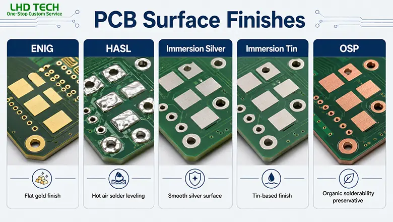
Understanding PCB Surface Finish Types
A PCB surface finish is a protective and functional coating applied to the exposed copper on a circuit board. These finishes generally fall into two main types:
- Metal-based finishes:
- Organic-based finishes:
- OSP (Organic Solderability Preservative)
The choice of a particular finish depends on how well it protects the copper, supports the soldering process, and provides the necessary electrical and mechanical performance for the final electronic assembly.
Why Surface Treatment Matters
Copper is prized for its conductive properties, but oxidation can degrade solder joint integrity, potentially causing failures during assembly or product operation. Surface finishes help to:
- Prevents copper tarnishing and corrosion.
- Preserves solderability (the ability for solder to adhere properly).
- Enhances shelf life and reliability.
- Ensures regulatory compliance with safe, lead-free, RoHS-conforming finishes.
PCB OSP Surface Finish Explained: The Organic Solderability Preservative

What is OSP in PCB?
OSP surface finish is an organic coating that forms a thin, clear, and effective protective layer against copper oxidation. It is applied through adsorption onto the copper surface: organic molecules bond with copper atoms, creating a uniform film on the PCB, ready for assembly.
This organic solderability preservative belongs to the azole family (typically benzotriazoles, imidazoles, and benzimidazoles), known for their chelating and anti‑corrosion capabilities. OSP is water‑based, making it the most environmentally friendly finish available, and it contains no heavy metals or hazardous substances.
Why Choose PCB OSP?
- Works well with high‑density, fine‑pitch pad layouts and advanced PCB designs.
- Offers a flat board surface, ideal for surface mount technology (SMT) processes and BGAs.
- Highly cost‑effective, making it an affordable choice for everything from high‑volume consumer gadgets to prototype PCBs.
How OSP Finish Works: Oxidation Protection and Solderability
A major issue after PCB manufacturing is the fast oxidation of exposed copper features (pads, vias, and traces). The OSP coating serves as an anti‑tarnish protective layer:
- Molecular adsorption: The organic coating molecules (usually from the azole family) are chemically adsorbed on the copper surface, producing a uniform, nearly invisible barrier layer.
- Oxidation protection: This film prevents moisture and oxygen from reacting with the copper, so the board can be safely stored, shipped, or handled without oxidation of copper.
- During the process of soldering: The OSP coating is designed to be easily removed by flux and heat, exposing a pristine copper surface for superior solder wetting and joint formation.
Example of Real OSP Performance
- Boards coated with OSP can maintain high solderability for months if stored at proper relative humidity and temperature. During reflow soldering, solder flux quickly removes the OSP film, and the solder spreads evenly across the newly revealed copper pad.
OSP Finish Process: Fabrication, Micro Etching, and Coating Steps
High-quality OSP application requires precision and strict process control:
OSP Surface Finish Process Steps:
- Cleaning: Removes oils, oxidation, and fingerprint residues.
- Topography enhancement (Micro Etching):
- Micro etching quantity is controlled to roughen the copper and aid OSP binding.
- Speeds of micro etching are tailored for optimal surface structure.
- Acid rinse: Often with sulfuric acid to neutralize and clear any last contaminants.
- Deionized (DI) water rinse: Removes all ions for a pure bonding surface.
- OSP coating (Film formation):
- The water-based OSP solution bath deposits an organic layer 0.2–0.5 µm thick.
- Final rinse and drying: Ensures a clean layer and no trapped moisture.
Advantages of OSP Surface Finish in PCB Manufacturing
OSP finish is popular among advanced board manufacturers for many reasons:
- Cost-effective: OSP is among the lowest cost surface finishes—perfect for high-volume, cost-sensitive production as well as prototype PCB runs.
- Environmentally safe: No hazardous metals, a simple manufacturing process, and lower environmental impact than other finishes.
- Superb flatness: OSP provides a board surface with zero “step” or unevenness—ideal for BGA, QFN, and high-pin-count ICs.
- Excellent solderability: When fresh, OSP yields superior solder wetting, allowing for reliable joints in high-speed SMT and reflow lines.
- Reworkable: Boards can be cleaned and re-coated if OSP is damaged or solderability is lost after long storage.
- Wide Compatibility: Works for rigid, rigid-flex, and even high layer count PCB builds. Many PCB manufacturers use OSP for fast-turn digital and communications products where flat surfaces and fine-pitch are critical.
Additional Benefits:
- Requires less aggressive flux than other finishes, simplifying the cleaning stage.
- Enables lower temperature soldering, minimizing PCB warping and component stress.
- Offers DFM (Design for Manufacturability) advantages—no complex layout rules are needed for boards coated with OSP.
OSP Surface Finish Advantages
| Feature | Why It’s Beneficial |
| Lower cost and simple process | Best value for high quantity, short lifecycle assemblies |
| Lead-free/eco-friendly | RoHS and WEEE compliant; water-based organic coating |
| Solderability (fresh) | Outstanding for modern SMT and prototype PCB work |
| Flat surface | No “dogbone” or step—for BGA/High-density ICs |
| Reworkable coating | Can recover unsolderable boards by re-coating |
Disadvantages and Shelf Life of OSP on Circuit Boards
No surface finish is perfect for every scenario—here’s where OSP finish reveals its limitations:
Limited Shelf Life:
- While cost-effective, the OSP coating can break down within 6–12 months of manufacture, especially in suboptimal storage environments (relative humidity above 70% or temperature over 30°C).
- Boards exposed after opening vacuum packaging quickly oxidize, especially if not assembled within 7–10 days.
Moisture/Handling Sensitivity:
- OSP is a thin, soft film. Improper handling, skin oils, or scratches during shipping/assembly can create oxidation “islands” and ruins solder wetting in localized areas of the PCB copper surface.
Multiple Reflow/High Temperature Limitations:
- OSP finish is not engineered for multiple reflow soldering or high temperature PTH (plated through-hole) soldering. The organic coating removes itself in the first reflow, potentially leaving copper vulnerable for additional solder cycles.
Inspection Challenges:
- The nearly invisible, transparent nature of the OSP layer makes QA and thickness inspection harder compared to the clear color cues of ENIG (gold) or HASL (dull white). Special wetting balance or solder dip tests are needed for aged PCBs.
Not Suited for Harsh or Long-Term Environments:
- For mission-critical electronics (defense, automotive, aerospace), OSP is generally not accepted for boards that will face moisture, temperature swings, or require storage for months or years before assembly.
OSP Shelf Life and Limitation Table
| Potential Problem | Typical Impact | Solutions/Workarounds |
| Short shelf life | Solderability loss after 6–12 mo | Assemble quickly; vacuum packaging; recoating |
| Handling scratches | Oxidation, poor solder | Handle with gloves; minimize manual contact |
| Heat cycles/excess heat | Finish breakdown | Limit reflows; opt for ENIG for multiple heats |
| Color change | Cosmetic; QC confusion | Test solderability; control micro-etch/OSP steps |
Common Issues with OSP Coating, Storage Conditions, and Handling
Key to OSP success is post-fabrication—even the perfect finish is easily ruined by improper storage, climate, or assembly habits.
Storage Requirements for OSP-Coated PCBs
- Vacuum Packaging: Immediately after OSP coating, circuit boards coated with OSP should be sealed with desiccant packs and a humidity card.
- Ideal Storage Conditions:
- Keep at 15°C–30°C temperature
- Maintain relative humidity between 30–70%, ideally at the lower end
- Assembly Best Practices:
- Assemble boards within 7 days of opening sealed bag to ensure a flawless process of soldering.
- Boards kept beyond shelf life may be recoated by cleaning and reapplying the OSP finish—ask your PCB manufacturer about this service.
Handling Precautions
- Use nitrile or cleanroom gloves at all times.
- Do not touch pad surfaces directly.
- Avoid compressed air from moist or oil-y house lines—dry filtered air only.
What if OSP Boards Look “Off”?
- Discoloration: A shift from shiny copper to brown or dull pink does not immediately mean lost solderability. Test with a solder dip and flux; if solder balls won’t wet the surface, the coating needs rework.
- Localized Oxidation: Usually a sign of storage bag puncture, failed desiccant, or high atmospheric humidity.
- Solder Dewetting: More prevalent over aged OSP, high micro-etching, or excess thickness. Confirm storage logs and request process data from your supplier.
Comparing OSP, ENIG, HASL, and Other PCB Surface Finishes
Choosing between OSP surface finish, ENIG, HASL, or alternative finishes depends on more than just price.
| Surface Finish | Relative Cost | Solderability Early | Max Shelf Life | Flatness | Reworkable | Lead-free? | Inspection Ease | Best For |
| OSP (organic solderability preservative) | Lowest | Excellent | 6-12 mo | Superior | Yes | Yes | Hard | Low-cost, high-density, fast-turn |
| ENIG (electroless nickel immersion gold) | Highest | Excellent | 12-24 mo | Superior | No | Yes | Easy | BGA, long shelf, rel-critical |
| Lead-free HASL | Medium | Good | 12-36 mo | Good | Yes | Yes | Easy | Mixed THT/SMT, moderate cost |
| Immersion Silver | Medium | Excellent | 6–9 mo | Superior | Limited | Yes | Easy | RF, signal, flex; short shelf |
OSP vs ENIG
- OSP finish provides better cost structure and flatness, whereas ENIG shines in shelf-life and long-term oxidation resistance.
- For projects with double or multi-stage soldering, ENIG or even lead-free HASL may offer more robust options than OSP.
When to Use OSP: Real-World Examples and PCB Capabilities
Best Scenarios for OSP
- Consumer Electronics: Phones, tablets, laptops, and routers, which require maximum design flexibility, fast assembly, and minimal cost.
- IoT and Communications: Gateways, modems, and sensors that rarely sit on shelves for long before assembly.
- Medical Disposables: Test modules or cards meant for one-time use or rapid-cycle products.
- Prototype PCB and Quick-turn Projects: The short time between production and assembly maximizes the soldering advantages while virtually eliminating shelf life concerns.
Key PCB Capabilities
- Fine-pitch component support
- Compatible with lead-free assembly
- Excellent for SMT-focused assemblies
When NOT to Use OSP
- Complex boards with multiple mixed assembly types and many high temperature wave soldering passes (many PTH parts).
- Defense, aerospace, or automotive boards where shelf-life and ultra-long reliability eclipse all else.
Expert Tips for Using OSP Surface Finish in PCB Manufacturing

- Request OSP Thickness Certification: Good PCB manufacturers will provide measured thickness logs for each production batch.
- Qualify Storage & Handling Chain: Confirm your distribution, storage, and assembly flows keep within temperature and humidity guidelines.
- Build in Test Coupons: Include extra, unused pads on each panel for solderability dip/wetting testing after storage.
- Use Controlled, Dry Assembly Environments: Place open OSP boards in dry cabinets (RH < 30%) if assembly scheduled over more than one day.
- Opt for Vacuum Repackaging if Assembly is Delayed: Your PCB supplier can usually re-vacuum package or even re-coat after aged storage.
- Document Finish Needs Clearly: Label “OSP surface finish (organic solderability preservative, RoHS)” in your Gerber/CAM notes.
- Ask About New OSP Chemistries: Some suppliers now offer new coating types of OSP with improved high temperature durability and longer unopened shelf life, making OSP viable for a wider range of devices.
Conclusion: Selecting the Right Surface Finish for Your Printed Circuit Boards
The OSP surface finish is a modern PCB copper surface treatment that balances cost-effectiveness, environmental safety, and superb initial solderability. For high-density, fast-turn, and consumer boards—especially those leveraging advanced SMT and prototype PCB flows—it’s unmatched for value.
However, its limited shelf life, handling sensitivity, and thermal endurance require close attention to storage, logistics, and assembly timing. If your production environment supports vacuum packaging, prompt assembly, and controlled relative humidity, OSP finish consistently delivers a cost-effective, lead-free, reliable solution for most circuit boards.
For PCBs exposed to multiple high temperature cycles, long shelf life, or mission-critical operation, finishes like ENIG (Electroless Nickel Immersion Gold) or lead-free HASL (Hot Air Solder Leveling) may be preferable—though at higher cost and possibly less planarity.
Ultimately, by partnering with your PCB manufacturer, specifying your precise requirements for finish, confirming process and shelf life data, and following best practices in storage and handling, you can take full advantage of the strengths of the PCB OSP surface finish while minimizing its drawbacks.
Frequently Asked Questions About PCB OSP Surface Finish
Q1: Can I combine OSP with other finishes for hybrid needs, like ENIG+OSP?
A: No – surface finishes are mutually exclusive on a given copper area. However, selective finishing is possible where some pads are OSP and others are ENIG/HASL, but it’s rare and increases cost/complexity. Always use Gerber/PCB CAM notes to specify.
Q2: How critical is OSP film thickness?
A: Critical! Too thin: copper is exposed, leading to early oxidation. Too thick: poor solder wetting. Most manufacturers target 0.2–0.5 μm. Ask for a certificate of conformance.
Q3: Does OSP interfere with test probe points?
A: For ICT (in-circuit test), OSP is generally acceptable—just ensure probe tips are sharp and pads aren’t oxidized. For pogo pin beds used over many cycles, avoid OSP as repeated contact can remove the film.
Q4: Are there PCB design changes needed for OSP?
A: Not in layout, but in production notes:
- Specify “OSP surface finish (RoHS)” in Gerber/ODB++ files.
- For DFM, avoid exposing large copper pour areas unless they are solderable, as OSP offers minimal long-term protection.
Q5: Is OSP good for flexible PCBs?
A: Yes, provided flexing after OSP deposition is minimized and handling protocols are strict. Vacuum packaging is even more critical here.
Q6: What’s the maximum number of reflow cycles before OSP degrades?
A: 1–2 cycles is optimal. Reliable vendors may claim up to 3, but test for your exact reflow profile and assembly flow.