Introduction
Whether you’re a beginner, hobbyist, or seasoned engineer, to build a prototype is an essential step in the circuit design and product development life cycle. The PCB prototype is two testing ground and springboard—it can letting creators explore, verify, and refine concepts before invest in mass production or a custom PCB. Without the risks or costs of a full-scale PCB manufacturing run, we can also prototype circuits, tweak board layout, experime with different designs, also debug issues in real time.
Prototype boards offer flexibility for both solderless and solder-based circuit building techniques. From solderless breadboard setups to soldering iron-tamed perf boards laden with ICs and custom connections, mastering these boards makes electronics accessible and scalable for any project.
When advancing from simple circuits to industrial designs, the practices for using prototype boards you develop here will empower you to reliably test everything from radio circuits to complex printed circuits and integrated circuits, before you invest in custom PCB fabrication or small-batch production boards.
What is a Prototype?
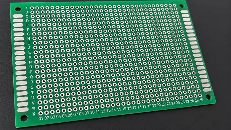
A prototype is a working early model of an electronic system. It tests concepts, catches design errors, checks functions and shows ideas to partners. It connects circuit schematics to finished PCBs and supports repeated design tweaks.
Why Prototyping Matters:
- Verification: Test the function of simple circuits and complex assemblies before scaling up for full PCB production.
- Cost Savings: Spot and solve layout, component, or soldering issues without costly errors on a custom printed circuit board.
- Learning Tool: To explore the operation of different types of prototype circuits—ideal for both new engineers and veteran designers.
- Speed: Rapid prototype shortens the design and test phase, letting you refine and optimize before custom board production.
Different Types of Prototype Boards
Understanding the different types of prototype boards can dramatically improve your workflow, letting you choose the right board for your prototype, from breadboards to PCB prototype boards and more.
| Board Type | Features & Advantages | Drawbacks | Best Use Cases |
| Solderless Breadboard | No soldering, good for beginners & rapid test cycles, reusable, ideal for simple circuits | Not for high-frequency/radio circuits. Connections are less secure than PCBs | Educational, temporary builds, prototyping |
| Perf board (Perforated Board) | Individual copper pads, custom wiring, perfect for one-off and irregular layouts—also called matrix board | Tedious wiring, possibility of solder bridges, not as neat as PCBs | Semi-permanent or one-off custom projects |
| Stripboard/Veroboard | Rows of connected copper strips, simplifies power & signal routing, ideal for demo boards or power busses | Must break copper strips for isolation, less flexible layout than perf board | Prototypes with repeated layouts or many busses |
| PCB Prototype Board | Professionally fabricated, double sided, can include surface mount components, closely matches production board | More expensive and slower than breadboard or perf board prototype; custom PCB design required | Small-batch runs; final prototype before mass production |
| Wire Wrap Board | “Wire wrap” connections: wire is wrapped around posts, robust but slow assembly, easy for modding or repairs | Bulky, less common in modern prototyping, replaced by soldered boards | High-reliability, legacy systems |
| Copper Clad Board | Solid copper over laminate, you etch your own copper traces—great for advanced prototyping or custom PCB early testing | Requires chemicals/tools for etching copper, less reusable | Custom circuit layout, RF circuits, surface mount prototyping |
More On Breadboards
A solderless breadboard is and ideal for solder-free circuit testing. Built-in spring clamps hold resistors, ICs and jumpers when plugged in, so you can rework circuits fast. It works great for early design trials, though it cannot handle long-term use or high-frequency signals.
Perfboard, Stripboard, and Veroboard
Perfboard (sometimes called perforated board, matrix board, or perforated circuit board) offers maximum flexibility. Each hole has its own isolated copper pad, making it possible to use through-hole components and connect components point-to-point with wires in any configuration.
Stripboard (also known as Veroboard) has copper strips that connect rows automatically. This board design makes it easy to build power and ground busses for simple to moderately complex circuits. You’ll often need to break strips at key points (using a drill bit) to avoid unintended connections—a technique called “track cutting” or “breaking copper strips.”
For radio circuits, analog test boards, or cases where you need robust, semi-permanent builds, perf boards and stripboards shine. Perf boards, in particular, are perfect for slightly more complex or irregular layouts, especially if you work with both analog and digital signals.
PCB Prototype Board and Beyond
When your prototype circuit reach its final form, or if you need to evaluate the real-world PCB assembly process, a PCB prototype board bridges the gap. A custom PCB prototype can be double sided, it can support surface mount devices (SMD), we can also use plated-through holes to closely mirror the final product.
Copper-clad boards are sometimes used by advanced designers who want to etch custom copper traces or experiment with board space-efficient prototypes. You can design and test unique layouts not possible with perf board or stripboards, or even mimic high-frequency production boards by maintaining a solid ground plane and minimal parasitics.
Benefits and Drawbacks of Prototype Boards

Benefits
- Rapid Implementation: Prototype electronic circuits in minutes or hours, rather than waiting days for a custom PCB.
- Zero-Risk Experimentation: Try new layouts, change parts, or swap ICs without solder on breadboard; with minimal risk on other boards if you use breakout or adapter boards.
- Lower Cost: Save money throughavoiding custom PCB orders until your design is validated.
- Educational Value: Prototyping electronic circuits helps visualize concepts, making it easy for students and hobbyists to explore and learn.
- Debugging: Spot design, solder, or layout errors and fix immediately—unlike with a production board where diagnose/repair is harder.
Drawbacks
- Signal Quality: Solderless breadboards add capacitance/inductance, making them unsuitable for high-speed digital or analog circuits.
- Physical Durability: Prototype boards—especially breadboards—aren’t rugged. For robust, mobile, or wearable projects, you need a printed circuit or at least soldered perfboard.
- Dense Designs: As your circuits get more complex, it’s easier to lose track of connections, or run out of board space on perfboard, stripboard, or breadboard.
- Surface Mount Limitations: Solderless breadboards and most perfboards aren’t natively suited to surface mount (SMD) components. SMD parts often require special adapter boards or a custom PCB prototype for proper assembly.
- Unintended Shorts: On perfboard, tight wiring and messy layout easily cause short circuits and solder bridges, particularly on dense or double-sided prototypes.
- Limited Ground Plane: Not like a custom PCB or etched copper-clad board, prototyping boards rarely provide a true ground plane, making analog or radio circuits more susceptible to noise and interference.
Even with these flaws, prototype boards suit design and testing well, cutting costly errors before PCB fabrication and mass production.
Components Used in Prototyping
The heart of any prototype circuit is its electronic components. To choose and handling these parts effectively can mean the difference between a working build and a frustrating debug session.
Essential Electronic Components for Prototyping:
| Category | Examples | Notes |
| Resistors | 1kΩ, 10kΩ, 220Ω, pull-up/pull-down | Use color-coded assortment packs for rapid prototyping |
| Capacitors | 0.1μF, 1μF, 10μF (electrolytic & ceramic) | Decoupling for ICs, stabilize power lines |
| Inductors | 10μH, 100μH | RF circuits, filters, power supplies |
| Diodes | 1N4001, 1N4148, LEDs | Power protection, signaling (use correctly aligned polarity) |
| Transistors | 2N3904, BC547, MOSFETs | Amplification, switching, logic |
| ICs | Op-amps, 555 timers, logic gates, microcontrollers (8051, ATmega328, ESP32) | Always check pinout/footprint for breadboard or perfboard use |
| Surface Mount Components | SOT-23, SOIC, QFN | Use SMD-to-DIP adapter boards, or migrate to custom PCB |
| Connectors | Pin headers, sockets, barrel jacks | Use solderable headers for flexibility |
| Switches/Sensors | Tactile pushbuttons, thermistors, photodiodes | Sensors often tested via breakout boards first |
| Displays | 7-segment, LCD, OLED | Some require breadboard or perfboard adapters |
Real-World Applications of Prototypes
Prototyping is central to PCB design. It lets makers, students and engineers build circuits, fine-tune layouts and revise samples prior to mass production.
Common Applications:
- Educational Projects: Breadboards and perf boards are mainstays in physics and engineering labs for building simple circuits, logic gates, and analog amplifiers and learning the fundamentals of circuit design.
- DIY and Maker Builds: Smart home controllers, robotics, IoT sensors, and even hobbyist radio circuits often start life as a prototype.
- Product Development: Before custom PCB layout and PCB manufacturing, professional engineers use prototype PCB boards and double sided PCBs to verify every function and workflow.
- Adapter/Breakout Boards: Use a breakout board for SMD-only ICs, making prototyping possible even when your component doesn’t fit standard perf board holes.
- Debugging and Repair: When production boards fail, prototyping boards are used to recreate, analyze, and repair circuits with speed and flexibility not possible on a custom printed circuit board.
Tools and Equipment: Setting Up Your Bench
The right tools make prototype building faster, safer, and far more reliable. Here’s what every serious prototyper needs:
Basic Tools
- Soldering Iron: Variable temperature for fine control; a must for perfboard, stripboard, or any prototype with soldered joints.
- Solder: Preferably lead-free. For finer joints, use thin gauge solder with rosin core for lower flux mess.
- Flux & Solder Wick: Essential for clean joints, fixing solder bridges, and reworking connections.
- Multimeter: Use for continuity checks, voltage, and verifying every prototype circuit section.
- Wire Cutters/Strippers: Vital for making neat, short, direct connections.
- Breadboard Jumpers: Color-coded for troubleshooting and organization on solderless boards.
- Tweezers: Precise placement of both through-hole and SMD components.
- PCB Holder/Helping Hands: For steady, safe soldering and placing small parts on your prototype board.
Advanced/Optional Tools
- Oscilloscope: To see waveforms and debug analog or mixed-signal prototype circuit boards.
- Logic Analyzer: For verifying digital signals and communications busses.
- Bench Power Supply: Adjustable voltage and current, with overcurrent (OCP) safety.
- Labeling & Organization: Label wires, busses, and test points for easier circuit board debug and future reference.
Design Process and Planning Your Prototype
Successful circuit prototypes start with planning. Skipping this can result in crowded, tangled boards and an endless debug cycle.
Design and Test Steps:
Start with a Schematic: We can use circuit design software (KiCad, Eagle, Altium, Fritzing) or pen and graph paper. Label each connection and value. This schematic is our blueprint—update it as customer’s make changes!
Choose Your Board Types: Choose from breadboard, perfboard, stripboard and PCB prototypes. Pick the board based on layout, signal speed, SMD needs, double-sided design, and whether you want fast solderless testing.
Plan Your Layout:
- Organize major blocks (input, processing, output).
- Keep power/ground busses clear and isolated from analog signals.
- On stripboard, pre-mark where you’ll need to break copper strips.
- On perfboards, group related components to minimize jumper length.
Simulate When Possible: Tools such as LT spice or Circuit Lab let you simulate performance, we can catch issues with simple circuits, also prepare for real-world build and test.
Prepare a Bill of Materials: Inventory every part—resistors, ICs, wires, connectors—before we start to solder or build.
Dry Run/Mock-up: Place everything on the board without solder (if possible). need to check, access, and logical wire routing.
Step-by-Step: Building Your PCB Prototype Board

Let’s take a deep dive into how to build and test a prototype circuit board, ensuring you follow the best practices for using prototype boards at every stage.
1. Lay Out the Schematic
Draw your prototype schematic, indicating where to place each component, including jumpers and adapter boards for any SMD or surface mount devices.
2. Prepare Your Board and Components
- For breadboard use, straighten leads and prepare plenty of jumpers.
- For perf board and stripboard, trim component leads and pre-bend as needed.
3. Insert and Place Components
- To start with ICs and sockets, then add passives (resistors, capacitors), also follo wthe connectors and switches.
- Orient everything for a logical workflow, respecting polarity and pinout. For veroboard, keep IC notches aligned.
4. Connect Components
- On a solderless breadboard, simply press leads and jumpers into the matrix.
- On perfboard, route point-to-point with wire or tinned copper wire. Use short, direct runs to avoid noise.
- On stripboard, solder directly to copper strips, then cut traces where needed to avoid accidental connections.
- When using a copper-clad board, etch the layout or use a Dremel to carve custom copper traces.
5. Make High-Quality Solder Joints
- Use a clean soldering iron tip, and heat both pad and lead for a reliable joint.
- Apply solder wick to absorb excess solder and clear bridges.
- Use flux for shiny, durable, low-resistance joints—especially on boards that oxidize (perforate areas).
6. Cut and Finish the Board
- Cut matrix, perf, or stripboard to size with a saw or score-and-snap technique. Smooth with a file to avoid sharp edges.
7. Check Continuity and Power
- Use a multimeter to ensure all expected connections and no shorts before applying power.
8. Power Up and Run Initial Tests
- Use a bench power supply with current limiting for your first power-on.
- Watch for unexpected heat, voltage spikes, or signal dropouts.
- Use a multimeter to confirm thevoltages at ICs, key busses, or connectors.
- If possible, we can test each block of our prototype boardseparately: verify regulators, clocks, micro controllers, or sensor modules are functioning in isolation before full system integration.
9. Debug and Refine the Prototype
- Perform systematic testing and troubleshooting for areas where the design and test process reveals faults.
- Probe test points and critical nodes to check for correct logic levels, analog waveforms, or digital bus activity.
- Check thecold solder joints, solder bridges, or open pads—common issues on perf board and strip board, especially with dense layouts.
Document, Iterate, and Prepare for Scale-up
- Update your schematic with all last-minute changes, jumper mods, or cut tracks you made during the prototyping process.
- Take clear photos (top and bottom, if double sided PCB or copper-clad) for future reference or sharing with collaborators.
- Annotate your layout, component changes, and any lessons learned.
- Keep all protoboard schematics and notes—this is invaluable when moving to production or custom PCB layout.
Best Practices for Using Prototype Boards

Stick to these prototype board rules to cut errors, save time and build reliable circuits:
Plan Your Layout First finalize your schematic and part placement. Keep signal traces short, cluster related parts, and leave room for troubleshooting.
Verify All Connections Test continuity with a multimeter after soldering. Check for shorts between copper tracks, mainly on veroboard and double-sided boards.
Use Separate Power and Ground Planes Set aside dedicated tracks for power and ground wherever you can. This lowers noise for analog and mixed-signal circuits.
Label and Color Code Avoid confusion by labeling rails, using colored jumpers, and even marking IC pin 1s and critical nodes directly on the prototype board.
Decoupling and Bypass Capacitors Place a 0.1μF ceramic capacitor close to every IC’s power pins—even on solderless breadboards—to filter transient spikes and prevent mysterious resets.
Shield Sensitive Circuits Separate analog and high-impedance wiring from switching power lines and high-speed digital traces. This matters greatly for radio and data acquisition prototypes.
Test in Stages Never troubleshoot the whole system at once. Test each individual subsystem before full assembly.
Use Breakout or Adapter Boards For pure SMD components, use breakout boards to convert SMD pins to through-hole pins, so they fit neatly on perfboards and breadboard.
Advanced Prototyping Techniques
Double Sided and Dense Layouts
- Some protoboards and all PCB prototype boards support double sided builds, allowing for more compact prototypes. Use wire jumpers or soldered pins as DIY “vias.”
- For very dense designs, it’s sometimes best to start with a copper-clad board and selectively etch or carve custom copper traces for your layout.
Surface Mount & SMD on Prototyping Boards
- Advanced users often glue down SMD ICs to a protoboard and use fine wire for “dead bug” prototyping, or mount the chip on an adapter/breakout board that’s easier to solder.
- Surface mount components save board space and are standard in most modern PCBs, but careful handling and fine soldering are needed for successful prototypes.
Wire Wrap for Prototyping
- Though less common today, wire wrap boards allow robust and easily modifiable connections for simple circuits or integrated circuits that use through-hole pins. Each wire is wrapped multiple times around gold-plated posts for solid, low-resistance contact—a method still used for some custom and high-reliability builds.
Matrix Board/Perforate Board Custom Techniques
- Perforated circuit boards (matrix boards) can be combined with tinned copper wire for point-to-point connections or even creative bus layouts. For very custom prototypes, “fly-wiring” above the board may be necessary for tight space or rapid changes.
Testing Signal Integrity and RF Layouts
- On prototype PCBs for radio circuits, always use short, direct traces, keep a solid ground plane underneath, and minimize unused copper to avoid stray capacitance—what works on a breadboard won’t always translate to stable, reliable radio performance.
FAQs About Prototyping and PCB Prototype Boards
Q: Are solderless breadboards reusable?
A: Yes. Solderless boards can be used thousands of times for simple circuits, perfect for beginners building and testing multiple designs.
Q: What’s the best prototype board type for analog signals?
A: For low noise, use a perf board or custom PCB prototype board; breadboards have too much parasitic capacitance for clean analog performance.
Q: I only have SMD parts. How do I use them on a breadboard?
A: Use a breakout board or adapter board to convert SMD pins to standard 0.1″ grid spacing for prototyping on breadboard or vero board.
Q: Can I use perf boards for mass production?
A: No, perf boards are for prototyping or small demonstrations. For production, use a custom PCB or custom printed circuit board for repeatability, durability, and proper component spacing.
Q: What is the advantage of a double sided PCB?
A: 2 Layer PCBs offer greater component density and easier routing, supporting more complex or compact prototype circuit boards.
Common Mistakes to Avoid
- Overcrowded Layouts: Insufficient board space leads to messy wiring, poor heat dissipation and tough troubleshooting.
- Skipping Decoupling: Missing power bypass capacitors near ICs causes unstable operation, especially for analog and MCU circuits.
- Misaligned or Backwards ICs: Double-check chip polarity before soldering onto perfboards or breadboards.
- Insufficient Solder Joints: Weak, cold solder joints will fail after temperature changes or physical handling.
- Neglecting Documentation: Failure to update schematics with on-board changes makes later PCB redesign extremely difficult.
- Not Testing Each Stage: Lack of step-by-step testing burns out components and lets basic design errors remain undiscovered.
Conclusion
Building and testing prototypes on a prototype board is the foundation of every great electronic project. Whether you’re a hobbyist prototyping simple circuits on a matrix board, a professional designing production boards, or an engineer using a PCB prototype board to validate a system before mass production, the principles remain the same: careful planning, disciplined layout, and vigilant testing.
From solderless breadboard test rigs to perforated circuit board assemblies, and on to modern double side pcb and custom printed circuit board builds, mastering the design process and best practices for using prototype boards ensures that your ideas not only work—but are ready to scale.