

Printed circuit boards (PCBs) are shrinking in size with every passing year, but their complexity and power density are increasing. Today, even a millimeter of board space holds value. This requires that pads, traces, component leads, and vias be placed precisely to ensure electrical integrity and space efficiency.
Inverter PCBs handle high voltages while converting DC to AC, so insufficient spacing increases risks. Without enough separation between conductive parts, electricity can jump across an air gap or leak along the board’s surface. Either problem can damage components and create a safety hazard.
PCB creepage and clearance requirements help engineers determine how much separation is needed between conductors at different voltages. The correct distances depend on operating voltage, insulation type, and environmental conditions.
This guide explains the relevant IEC standards and the key factors that affect PCB spacing, along with practical layout and manufacturing considerations.
What Are Creepage and Clearance Distances?
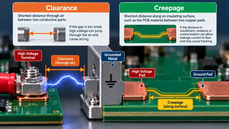
Creepage and clearance distances describe the separation between conductive parts in a printed circuit board (PCB), but they measure different paths.
Clearance is the shortest distance through air between two conductive parts. For example, the gap between a high-voltage terminal and nearby grounded metal. If this gap is too small, high voltage can cause electricity to jump through the air and trigger arcing.
Creepage is the shortest distance along an insulating surface, such as the PCB material between two copper pads. If this distance is insufficient, moisture or contamination on the surface can allow leakage current to flow and may cause electrical tracking.
| Feature | Clearance | Creepage |
| Measured through | Air | Insulating surface |
| Main concern | Electrical breakdown or arcing | Surface leakage and tracking |
| Key influences | Impulse voltage, insulation type, altitude | Working voltage, pollution degree, material CTI |
| PCB example | Air gap between terminals | Surface path between copper pads |
The PCB clearance and creepage distances may look similar on a flat PCB. However, the paths can differ around components/slots and other physical features.
Engineers must check both requirements separately. Under IEC 60664-1, the applicable creepage distance must also satisfy the associated minimum clearance requirement.
Why These Distances Matter in Inverters
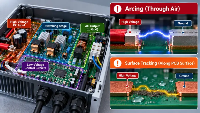
Take the solar inverter as an example. It usually has a high-voltage DC input, a switching stage, and an AC output connected to the grid. Managing these AC and DC circuits on a PCB requires careful electrical separation, especially where low-voltage control circuits sit near power components.
Insufficient spacing creates two main risks:
- Arcing: A voltage surge can cause electrical breakdown through the air between conductors.
- Surface tracking: Moisture and contamination can encourage leakage current along the PCB surface. Over time, conductive paths may develop.
A failure could damage power components and interrupt inverter operation. It can also compromise protection against electric shock. Correct insulation spacing helps reduce these risks throughout the equipment’s service life.
Which Standards Apply to Inverter PCB Spacing?
The applicable safety standard depends on the inverter’s purpose and intended market.
| Standard | Application |
| IEC 60664-1 | General insulation coordination, including creepage, clearance, and solid insulation |
| IEC 62109-1 and IEC 62109-2 | Safety requirements for photovoltaic power conversion equipment and PV inverters |
| IEC 62477-1 | Safety of power electronic converter systems |
| IEC 61800-5-1 | Safety of adjustable-speed electrical power drive systems |
IEC 60664-1 provides the general foundation. Its scope covers equipment rated up to 1,000 V AC or 1,500 V DC, with frequencies up to 30 kHz. That frequency limit matters in modern inverter circuits. Where insulation is exposed to periodic voltage stress above 30 kHz, IEC 60664-4 provides additional requirements for frequencies up to 10 MHz.
Engineers should begin with the relevant end-product standard because it may contain specific insulation rules. The edition accepted by the target market also needs confirmation, especially when standards have recently been revised.
Main Factors That Determine Creepage and Clearance Requirements
Before calculating PCB creepage and clearance distances, engineers need to establish the inverter’s electrical and environmental conditions.
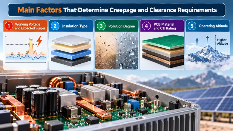
1. Working Voltage and Expected Surges
Working voltage is the voltage across an insulation barrier during normal operation. The DC-link voltage inside an inverter may exceed its nominal input voltage, so each barrier must be assessed individually.
Clearance also depends on transient voltages. The applicable standard uses factors such as system voltage and overvoltage category to determine the required impulse withstand voltage.
For example, some grid-connected PV inverter certifications specify Overvoltage Category II for the PV input and Category III for the AC mains connection. These classifications depend on the equipment and installation. Therefore, designing around nominal voltage alone can leave insufficient clearance during a surge.
2. Insulation Type
The spacing also depends on the protection each insulation barrier must provide.
- Functional insulation: Separation needed for the circuit to operate correctly.
- Basic insulation: Provides basic protection against electric shock.
- Supplementary insulation: An independent protective layer added to basic insulation.
- Reinforced insulation: A single insulation system providing protection equivalent to double insulation.
Reinforced insulation generally has more demanding requirements than basic insulation. So, the barrier between hazardous power circuits and accessible control interfaces may require reinforced insulation in an inverter, depending on the equipment’s protection scheme.
3. Pollution Degree
Dust and moisture can affect how electricity travels along an insulating surface. IEC standards classify these environmental conditions into four pollution degrees.
| Pollution Degree | Typical Conditions |
| PD1 | No pollution or only dry, nonconductive pollution |
| PD2 | Mainly nonconductive pollution, with occasional temporary conductivity caused by condensation |
| PD3 | Conductive pollution, or nonconductive pollution that becomes conductive through expected condensation |
| PD4 | Persistent conductivity caused by conditions such as conductive dust, rain, or snow |
Some PV inverter certifications specify PD2 for protected indoor conditions and PD3 for more exposed environments. However, outdoor installation does not automatically mean PD3. Engineers must evaluate the environment around the PCB, including the protection provided by the enclosure.
4. PCB Material and CTI Rating
The comparative tracking index (CTI) indicates how resistant an insulating material is to surface tracking under specified test conditions.
Materials with higher CTI values generally permit shorter creepage distances under otherwise comparable conditions.
| Material Group | CTI Value |
| Group I | 600 or higher |
| Group II | 400 to below 600 |
| Group IIIa | 175 to below 400 |
| Group IIIb | 100 to below 175 |
Conventional FR-4 materials often belong to Group IIIa, although their exact classification varies. Check the laminate supplier’s specifications before selecting a material group. Component packages may also use insulating materials with different CTI ratings.
5. Operating Altitude
Air becomes less dense at higher elevations, which reduces its electrical breakdown strength. IEC 60664-1 specifies clearance requirements for use up to 2,000 meters and provides correction factors for higher altitudes. For example, the clearance correction factor at 5,000 meters is approximately 1.48 relative to the 2,000-meter baseline.
Creepage distances are usually not multiplied by the same altitude factor. However, the final creepage distance must still satisfy the corrected clearance requirement. This matters for inverters installed at high-altitude solar sites, where larger air gaps may be necessary.
How to Determine the Required PCB Creepage and Clearance Distances
After the operating conditions are established, engineers can calculate the required PCB creepage and clearance distances using the applicable standard.
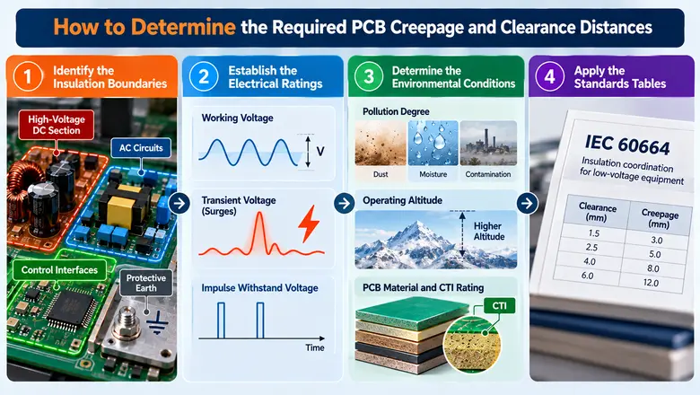
Step 1: Identify the Insulation Boundaries
Mark the circuits that must remain separated, including the high-voltage DC section, AC circuits, protective earth, and control interfaces. Classify each boundary according to its insulation function.
Step 2: Establish the Electrical Ratings
Determine the working voltage, along with expected transients and required impulse withstand voltage. Check whether IEC 60664-4 also applies to circuits exposed to high-frequency voltage stress.
Step 3: Determine the Environmental Conditions
Identify the pollution degree, maximum altitude, and CTI group of the actual insulating materials.
Step 4: Apply the Standards Tables
Use the relevant tables to determine the required PCB clearance and creepage distances. Apply the appropriate insulation classification and altitude correction, then check that the final creepage meets or exceeds the corrected clearance.
A Real Inverter Design Example
Let’s look at a real example to understand how creepage and clearance distances change with the type of insulation.
Texas Instruments’ TIDA-01456 reference design provides a useful example for a three-phase industrial inverter. The design uses Overvoltage Category III and Pollution Degree 2 conditions, with the following spacing requirements:
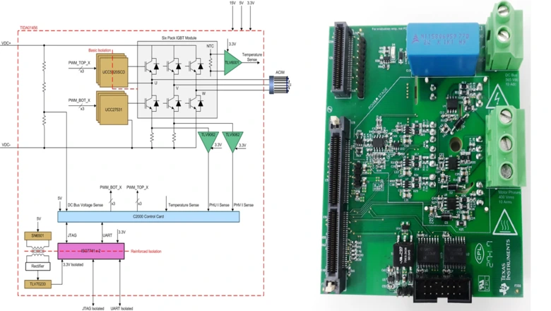
| Insulation Type | Clearance | Creepage |
| Basic | 3 mm | 4 mm |
| Reinforced | 5.5 mm | 8 mm |
Notice how reinforced insulation needs much more space. In this design, reinforced insulation is used at the communication interface to provide greater protection between circuits. Other parts of the inverter use basic insulation where appropriate.
This example shows why engineers must identify the required insulation type before deciding how far apart components should be placed.
Note: These values illustrate how insulation classification affects layout. They belong to that particular design and its referenced standard edition, so they should not be applied directly to other inverters without checking current requirements.
PCB Layout Practices for Maintaining Safe Spacing
Correct calculations are only useful when the finished PCB and assembly preserve the required creepage and clearance distances.
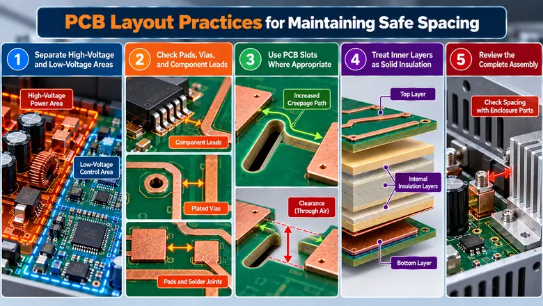
1. Separate High-Voltage and Low-Voltage Areas
Keep high-voltage power components away from low-voltage control circuits where practical. Check the spacing around MOSFETs, IGBTs, DC-link capacitors, and gate-driver connections. Exposed copper and grounded mounting hardware also need attention.
2. Check Pads, Vias, and Component Leads
Spacing problems often occur around component footprints. A trace may meet the required distance, but an exposed pad, plated via, or solder joint creates a shorter path. Use actual component dimensions when reviewing the layout.
Allow for fabrication tolerances as well. Hole positioning, routed edges, and component placement can affect the available separation.
3. Use PCB Slots Where Appropriate
A routed slot can increase creepage distance by making the surface path longer. However, its effectiveness depends on the slot dimensions and pollution degree. IEC 60664-1 specifies minimum groove widths that affect how the creepage path is measured.
A slot may leave clearance unchanged because electricity can still cross the opening through air. Check both distances after adding a slot, and confirm that the opening will not weaken the PCB mechanically.
4. Treat Inner Layers as Solid Insulation
The separation between copper on different PCB layers follows different rules from surface creepage. For multilayer boards, the insulating material between internal conductors must satisfy the applicable solid-insulation requirements. This makes dielectric thickness and material selection important during PCB stackup design.
5. Review the Complete Assembly
Spacing can change when the board is installed inside an inverter. Mounting screws, heatsinks, metal brackets, and nearby cables can introduce shorter electrical paths.
For example, a grounded heatsink close to a high-voltage terminal may reduce clearance even when the bare PCB layout meets its requirements. Review the final mechanical arrangement before approving the design.
Common PCB Spacing Mistakes to Avoid
Even when the initial calculations are correct, several design mistakes can compromise insulation:
- Using nominal voltage alone: Working voltage and expected surges are overlooked.
- Ignoring component footprints: Pads, leads, and solder joints reduce the finished spacing.
- Relying on solder mask: Ordinary solder mask is treated as qualified insulation without supporting evidence.
- Assuming PD2 applies everywhere: Actual moisture and contamination conditions are overlooked.
- Applying altitude corrections incorrectly: Clearance is increased, but its relationship with creepage is missed.
- Checking only the bare PCB: Heatsinks and mounting hardware introduce new conductive surfaces.
These problems are easier to correct during layout review than after PCB fabrication and assembly.
How to Verify Spacing During Manufacturing
Verification starts with comparing the layout against the approved insulation requirements. Engineers should inspect the shortest air and surface paths, including component leads, copper features, slots, and nearby mechanical parts.
Depending on the inverter’s safety standard, the verification process may include:
- Dimensional inspection: Checks critical gaps, slots, and component placement.
- Optical inspection: Identifies solder bridges and visible assembly defects.
- Dielectric withstand testing: Evaluates insulation under a specified test voltage.
- Insulation resistance testing: Measures resistance between separated conductive parts.
- Partial-discharge testing: Applies where required, including qualifying Type 2 protection.
The team must also factor manufacturing cleanliness. Flux residue and other contamination can affect surface insulation in humid environments.
Automated optical inspection can support assembly quality checks, while bare-board testing helps identify electrical manufacturing defects. Make sure that the testing and dimensional inspection both follow the product’s approved qualification plan.
Conclusion
Creepage and clearance requirements need attention early in inverter PCB design. Once the layout becomes crowded with power components and control circuits, correcting insufficient spacing can mean moving components or changing the board dimensions. Checking these distances against the applicable standards during design can save considerable rework later.
A right PCB manufacturing partner can review the design before production and identify potential fabrication challenges. LHD TECH offers PCB fabrication and assembly services, with engineering support for reviewing board layouts, copper spacing, material choices, and manufacturing feasibility. Its capabilities also include heavy copper PCB manufacturing for demanding power electronics applications.
Have an inverter PCB ready for production? Send LHD TECH your Gerber files and BOM to get technical feedback on your design and request a manufacturing quote.