Introduction to BGA Solder, BGA Rework, and PCB Assembly
At LHD TECH, we are well aware that the world of BGA soldering process technology, PCB assembly and SMT assembly is precisely the forefront where innovation and reality interweave. It is precisely because of the advanced soldering technology – especially the breakthroughs in circuit miniaturization, reliability and high-speed performance of ball grid array (BGA) technology – that modern electronic products have become a reality. So, why are BGA, BGA solder balls and BGA rework processes so crucial? How do engineers precisely complete the mounting of a specific BGA chip, manage hundreds or even thousands of tiny solder balls on the chip, and ensure that every solder joint is perfect both electrically and mechanically?
In this guide, LHD TECH will take you through a comprehensive understanding: from the preparation of stencil and PCB pads, reflow soldering, full board operations, to advanced BGA rework processes, ball placement techniques, as well as the tools and techniques trusted by professionals.
What is BGA? Understanding Ball Grid Array and Soldering Techniques
Ball Grid Array (BGA) technology represents a revolutionary advancement in the field of integrated circuit packaging. BGA is densely packed with tin balls at the bottom of the chip package, serving as a bridge between the chip and the PCB board, conducting electrical signals and providing fixed connections. BGAs are integral to today’s high-performance designs, including CPUs, memory chips, and wireless modules.
Why Use Ball Grid Array (BGA) in Modern PCB Assembly?
- High Pin Density: Compared with pin-enabled or QFN pin-free packages, BGA can form more connection points and has a higher density.
- Electrical & Mechanical Connections: The chip is soldered onto the PCB through solder balls, which is both conductive and fixed.
- Signal Integrity: The internal connection path of BGA is short and the parasitic inductance is low, making it suitable for high-speed circuits.
- Thermal Performance: The tin balls at the bottom of the BGA are miniature heat pipes and heat dissipation blocks.
- Surface-Mount Compatibility: BGA is compatible with SMD and SMT production lines and is specially designed for large-scale manufacturing.
Structure of BGAs and the Importance of Stencils & PCB Pads
Anatomy of a BGA Chip
- Die/Chip Core: The silicon IC.
- Substrate: Provides routing and mechanical support.
- Array of Solder Balls: Arranged in a precise matrix, typically 0.5 mm pitch or greater.
- Encapsulation: For protection against moisture and handling.
Importance of Stencil in SMT Assembly
Stencils controls the solder paste to be printed onto the PCB pads. The holes on the steel mesh are customized according to the size and spacing of the solder balls of each BGA chip to match the amount of solder paste. There is too little solder paste and poor contact. Too much solder paste leads to solder bonding or voids.
PCB Pads and BGA Pads: The Foundation of Good Solder Joints
- BGA pads on the circuit board must be clean, flat, and free of oxidation.
- Non-solder mask limited pads (NSMD), as this design enables a stronger and more reliable connection between the pads and the solder balls.
Understanding the BGA Soldering Process: Step-by-Step SMT Assembly and Reflow

BGA soldering process not only heats and melts the solder balls, but also involves a complete set of interlocking processes to ensure the reliability of the solder joints.
SMT Assembly Steps for BGA Soldering
- Stencil Printing: The steel mesh is formed by laser cutting or electroforming. The solder paste is printed onto the pads of the PCB with a scraper to match the solder paste with the array of solder balls at the bottom of the BGA.
- Placing the Component: Use tweezers or a vacuum pen to pick up the BGA chip and place it in the correct position on the corresponding pad of the solder ball.
- Reflow Soldering: The boards are sent into a reflow soldering furnace or hot air soldering table with precise temperature control. After the tin ball melts, the chip will be automatically straightened by the surface tension, forming a “self-centering” effect.
- Cooling: Control the cooling speed, neither too fast nor too slow.
- Inspection: Use X-rays to detect whether there are hidden soldering defects of BGA.
How to Clean the PCB: Ensuring Reliable BGA Solder Joints
A clean printed circuit board (PCB) is essential before and after BGA soldering.
- Initial Cleaning: Before printing solder paste, clean the PCB pads with isopropyl alcohol (IPA) and a lint-free cloth.
- Clean Between Steps: After removing the BGA, use solder tape to clean up any remaining flux.
- Post-Solder Cleaning:The bottom of the BGA on the board with high reliability requirements should be cleaned with ultrasonic waves or gas phase to ensure reliability.
- Drying: After cleaning, make sure the PCB is completely dry before proceeding to the next step.
Advanced Soldering Techniques & Tools: From Hot Plate to Rework Stations

Soldering a BGA can involve various tools and methods:
Tools of the Trade
- Hot Plate or Preheater: The entire board should be preheated evenly first to prevent thermal shock damage to the board during heating.
- Hot Air Soldering Station: It is very convenient to disassemble and assemble a certain BGA chip separately by using local reflow and rework.
- Reflow Oven: Professional SMT assembly lines provide controllable and repeatable temperature curves for the entire board. The reflow soldering furnace is programmed with the holding zone, heating zone and reflow zone to ensure the perfect melting of the solder balls and protect the sensitive components.
- Desoldering Braid (Solder Wick): Remove the removed chips to suck away the excess old solder or residual solder dross on the BGA pads and PCB pads.
- Advanced Rework Stations: These combine bottom-side preheating with precise top-side hot air flow and vision alignment systems. Some feature split-vision cameras to align the chip to the paste, ideal for 0.5 mm pitch BGA or finer.
- Tweezers or a Vacuum Pickup Tool: For accurately placing the component or handling delicate BGAs during the bga rework process.
- Stencil Printer: Print the solder paste evenly and defect-free onto the corresponding pads of the BGA chip.
Soldering Techniques for Ball Grid Array (BGA) Components
- Lead-Free Solder: Lead-free solder complies with RoHS environmental protection requirements. The most commonly used one is SAC305, but the reflow temperature is 10 to 20 degrees Celsius higher than that of traditional lead-containing solder – board warping and deformation of the board are strictly prohibited.
- Flux and Solder: During the BGA soldering process, the selection of highly active and low-residue fluxes can improve the wettability of the solder.
- Paste to the Chip before Placement: When disassembling the machine or when the solder ballsoxidize, for repair or ball planting, apply solder paste on the solder balls of the BGA to make the connection more reliable.
Precision with Reballing and the BGA Rework Process
When Is BGA Rework or Reballing Needed?
- Failed X-ray or electrical test after SMT assembly
- Defective circuit requiring chip replacement
- Upgrading or recycling valuable BGA chips (like CPUs or FPGAs)
- Soldering defects—bridging, head-in-pillow, or misalignment
The BGA Rework Process Explained
- Remove the Faulty BGA Chip
- First, preheat the PCB with a hot plate or a bottom heater.
- Then, use a hot air soldering table or an infrared heating tool to locally heat the chip to melt the solder.
- Vacuum suction to lift the BGA chip – do not pry hard to protect the pads.
- Clean the Pads (and the Chip)
- Use solder pads and flux to clean the old solder at the bottom of the PCB pads and chips.
- Inspect under a microscope for pad lift or damage.
- Reballing the BGA
- Secure the BGA in a reballing fixture.
- Place a steel mesh stencil matched to the chip pitch over it.
- Put the solder balls into each opening, apply flux and fix the solder balls.
- Gently heat with a heating plate or a small reflow furnace. After the solder balls melt, the soldering is completed. After cooling, clean thoroughly.
- Attaching New Solder and Chip Placement
- Apply fresh paste to the target PCB pads with a stencil.
- Align the chip using an advanced rework station or vision system; precise centering is critical, as the tension of the molten solder during reflow will self-align, but only within a narrow margin.
- Reflow the New BGA
- Reflow soldering using a controlled temperature profile or hot air tool.
- Inspect (X-ray) after cooling for correct joint formation and absence of defects.
Tips for Reballing Success
- Always match ball size and alloy to the original manufacturer spec (e.g., 0.5 mm pitch BGA may require 0.3 mm solder balls).
- Keep humidity controlled: moisture-sensitive BGAs should be pre-baked to avoid “popcorning.”
- Practice on scrap boards before handling expensive ICs or crucial assemblies.
Solving Common Soldering Defects in BGA and SMT Assembly
Even with perfect technique, BGA soldering and rework pose unique challenges. Here are prevalent issues and solutions:
| Defect Type | Cause | Solution/Prevention |
| Voids | Trapped flux, excessive paste, moisture | Use lower-residue flux, pre-bake, adjust reflow profile |
| Head-in-Pillow (HiP) | Pads oxidized, paste dried, uneven heating | Clean pads, use active fresh flux, optimize soak phase |
| Bridging | Excess paste, misplacement | Adjust stencil aperture, increase placement precision |
| Open Solder Joints | Insufficient paste, excessive warping | Ensure correct volume, use thicker PCBs if needed |
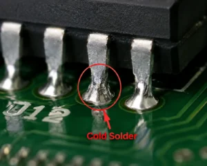
| Cold or Brittle Joints | Cooling too fast, incomplete reflow | Use controlled cool-down profile, proper time above liquidus (TAL) |
| Pad Lift/Delamination | Overheating during rework, repeated reflow cycles | Limit rework attempts, use precise temp tracking |
Professional Tips for BGA Soldering, Reflow, and Circuit Rework
- Use Advanced Rework Stations: A precision and valuable chip, a rework system that uses a beam splitting prism for alignment and closed-loop temperature control.
- Moisture Control Matters: BGA should be stored dry and baked before use.
- Documentation: Record the temperature curve and rework parameters as the data basis for tracing back to the source.
- Quality over Quantity: When assembling complex PCBS, try to complete the rework in one go.
- Routine Maintenance: The hot air welding table and the steel mesh printing machine should be cleaned and calibrated regularly.
Applications of BGA Technology in Modern PCB Assembly
BGA is ubiquitous in electronic products ranging from mobile phones and routers to servers and autonomous driving modules.
- Smartphones/Tablets: SoC (System-on-Chip), memory, power management chips and various sensors all adopt high-density BGA with a pitch as small as 0.4mm or even 0.5mm.
- Computing: For CPU, GPU and memory chips, BGA can ensure that they achieve a higher number of I/ OS and better heat dissipation performance.
- Automotive: BGA makes the electronic control unit and sensor module both reliable and shock-resistant.
- Industrial/Medical: The equipment operates in harsh or mission-critical environments, and BGA ensures stability.
- Emerging Tech: For 5G, Internet of Things (IoT), and AI edge devices, to adapt to small size and low power consumption, small BGA is selected.
Comparison: BGA vs Other Solder Packages and Soldering Techniques
BGA vs. QFP vs. QFN:
| Feature | BGA | QFP | QFN |
| Pin Count | 100–2000+ | Up to ~200 | Up to ~100 |
| Solder Connections | Array of solder balls | Gull wing leads | Bottom pads |
| Inspection | X-ray, electrical test | Visual, microscope | Visual, microscope |
| Thermal Management | Excellent | Good | Good |
| SMT Assembly Line | Preferred | Suitable | Suitable |
| Soldering Process | Reflow, highly precise | Hand/automated, easier | Hand/automated |
Packaging operations like QFP and QFN are simple. However, when it comes to applications with high complexity and high-speed signals, the performance of the BGA soldering process is much better. Moreover, single BGA has higher requirements for detection methods and temperature curve control.
Frequently Asked Questions (FAQ): BGA Soldering Process, PCB Assembly, and Rework
Q: Can I use a hot air soldering station to repair a BGA at home?
A: Sure. First, preheat the entire board with a heating plate or a preheater, and then monitor the temperature.
Q: What is the secret to a reliable BGA solder joint?
A: The pads should be cleaned thoroughly, the amount of solder paste should be moderate, the placement should be accurate, and the reflow curve should be verified to ensure that the solder balls can wet both the chip pads and the PCB pads. Use high-quality flux and conduct X-ray or on-off tests to identify potential hazards.
Q: What is reballing in the context of BGA rework?
A: Remove the old and faulty BGA, clean the pads on the chip and PCB thoroughly, and reattach new solder balls to the bottom of the chip with a steel mesh and flux, then reattach them back to the board and pass through reflow soldering.
Q: When should I use lead-free solder for BGAs?
A: Lead-free solder (SAC305) complies with RoHS environmental protection requirements. It is commonly used in commercial and industrial electronic products. It should be noted that the reflow temperature of lead-free solder is higher, so it is necessary to prevent the board from warping and avoid excessive thermal stress.
Q: Is it necessary to X-ray every BGA during pcb assembly?
A:Samples of products with high reliability and high pin count. With good process control and functional testing, X-ray inspection is the gold standard for discovering hidden solder joints or solder connections.
Q: What kinds of soldering defects are most common with BGAs?
A: BGA soldering defects that are prone to occur due to incorrect reflow curves, incomplete cleaning, and insufficient steel mesh precision include voids, solder bonding, pillow effect (HiP), pad cracking, as well as cold soldering or brittle solder joints caused by insufficient reflow.
Q: What is the role of flux in BGA solder and rework?
A: The main function of flux is to promote wetting, prevent oxidation, and help the solder balls melt normally, thereby forming A strong electrical and mechanical connection between the chip pads and the PCB pads.
Q: Can hobbyists or engineers solder BGAs on a hot plate or with a hot air gun?
A: Yes. First, practice on a waste board and closely monitor the temperature of the board throughout the process. The key is to preheat thoroughly, keep your hands steady and align accurately. It will be much easier to place the chip with tweezers or a vacuum pen.
Conclusion: BGA Solder, Rework, and Reliable PCB Assembly for the Future
In LHD TECH’s view, the welding and rework process of BGA has now become an indispensable part of the manufacturing of high-end electronic products – whether it is smartphones, laptops, medical equipment, automotive systems, or even aerospace applications, none of them can do without it. Mastering a complete set of BGA soldering processes, including: designing a reasonable steel mesh to ensure precise solder paste printing onto PCB pads, precise surface mount technology, impeccable reflow soldering temperature curve control, and proficiently completing ball placement when necessary – these are no longer “elective courses”, but basic skills.
Key Takeaways:
- Professional tools on the SMT assembly lines: hot air soldering table, steel mesh printing machine, X-ray inspection system… It is precisely they that ensure fast, stable and high yield in production.
- From cleaning the PCB to surface mount alignment and monitoring the reflow process – each step determines the electrical and mechanical reliability of each BGA.
- High-end rework workstations, lead-free solder alloys, and the appropriate selection of fluxes are all key points in the process. For the high-density design with a 0.5mm spacing, the surface tension of the molten tin is as important as the quality of the solder paste and the rate of temperature rise, and none of them can be missing.
- Both new products and repair parts need to master advanced welding techniques, be familiar with common defects, and be able to use solid detection methods. All these can make prototype verification smoother, debugging faster, and the cost of on-site fault repair lower.
In our management, whether it’s professionals, DIY engineers, or maintenance technicians, being able to make BGA solder joints flawless is not only a technical challenge but also a genuine sense of achievement. The skills and insights discussed in this guide are precisely designed to help you handle the various requirements of the next generation of electronic design and SMT assembly with ease.