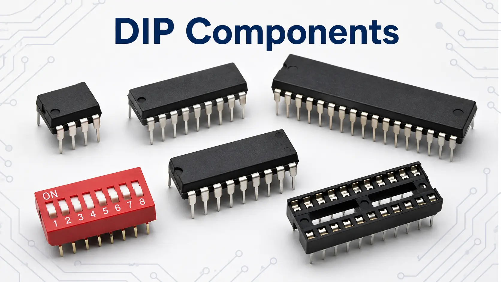
Introduction to DIP Package
The DIP package, short for Dual Inline Package, is foundational to electronics. Whether you’re a student on a breadboard, a repair technician, or a circuit designer, chances are you’ve worked with a DIP or two. The dual in-line package is easy to identify: a rectangular package body with two rows of pins extending from each longer side. This design made it integral to prototyping, mass manufacturing, and repair of printed circuit board assemblies for over half a century.
Why is the DIP package so important?
- It embraces simplicity in insertion, inspection, and replacement.
- DIP ics and dip components drove the mass adoption of IC technology, with the 555 timer and logic chips as icons.
- The features of dip packages—durability, accessibility, and standardized pin spacing—keep them relevant in modern industry, prototyping, consumer electronics, and educational labs.
What is a Dual Inline Package (DIP)?
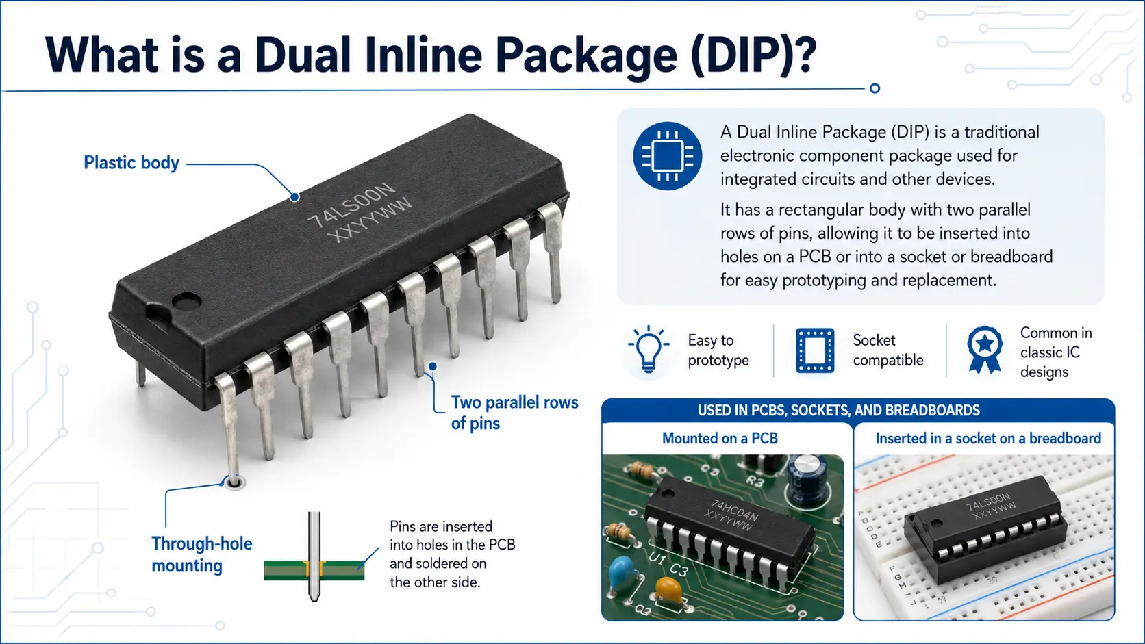
A dual inline package (DIP) or dual in-line package (sometimes called “DIL package”) is a component package with two parallel rows of pins. The dip pin leads emerge perpendicularly from each side of the rectangular package body and are spaced at a consistent pin spacing—most commonly 2.54mm (0.1”). The number of pins can vary—common dip package standards range from DIP8 to DIP40, but larger pin counts such as up to DIP64 are available.
The DIP format is a type of dip package that serves as a bridge between the silicon die inside and the rest of the electrical circuit on the pcb or circuit board. Its robust package substrate, molded from plastic or ceramic, protects the internal components yet is easy to manufacture and install in various package types.
Key characteristics—“Features of DIP” analog:
- Rectangular package body with two rows of pins
- Each row of pins is spaced precisely for international compatibility
- Polarity identification notch in the package for correct orientation (Pin 1)
- Pins can be inserted into a socket, breadboard, or through-hole in a pcb
Understanding DIP means grasping its role as both a mechanical and electrical link between integrated circuit and the wider world—still essential in prototyping and legacy support.
A Brief History of the DIP Package
The first dip originated in the 1960s when Fairchild introduced this new ic package design to streamline the assembly of increasingly complex integrated circuits. Prior to this, the “can” (TO-5) or flat-pack packages were cumbersome, limited by their pin configuration and spacing, and failed to support the rapid scaling in digital electronics.
The dual in-line package set the world standard:
- It became the electronically and mechanically robust solution for ICs in consumer and industrial electronics alike.
- As demand grew, JEDEC established standards for row width, dip pin dimensions, and pin spacing, supporting international markets.
- By the 1970s and 80s, the dip format dominated computers (Commodore 64, Apple I), industrial controls, and test equipment.
- Even now, new ic’s are sometimes available in dip format for specialty and educational needs.
Features and Structure of DIP Packages
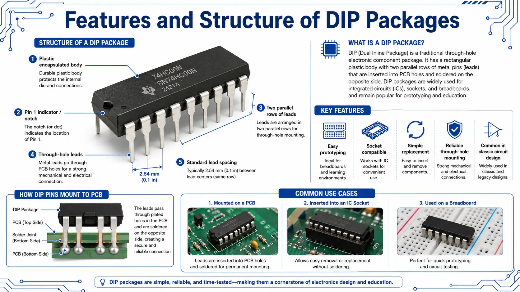
Understanding the structure and features of dip packages is essential for working with and designing with this package type.
Main Structural Elements:
- Silicon Die: The actual “chip” inside the dip package
- Package Substrate: Supports the die and contributes to the overall strength of the package
- Lead Frame and Dip Pins: Metal structure connecting the chip to the external environment; provides electrical connections
- Plastic or Ceramic Mold (package body): Encases and protects the die and wire bonds
- Wire Bonds: Performed during dip package assembly, connecting die to the lead frame
- Identification Notch of the DIP: A notch or dot marks Pin 1, critical for proper insertion and function
There are different types of dip package, including:
- PDIP (Plastic Dual In-Line Package): The most common, durable and cost-effective for most consumer electronics and prototyping contexts.
- Ceramic DIP (Ceramic Dual In-Line Package): Used in applications demanding higher temperature tolerance or specific features, such as windowed UV erasable ROMs.
- Shrink DIP and Skinny DIP: Offer reduced package width or size of the dip package for denser layouts, maintaining standard row spacing for compatibility.
- Wide DIP: Used when increased package width is needed for higher pin count or special thermal concerns.
Features of dip packages:
- Clear pin orientation via notch in the package
- Internationally accepted dip form standards (JEDEC)
- Packaging supports both hand and automated assembly
Common Dip Package Table Example:
| DIP Type | Package Size | Number of Pins | Pin Spacing | Notes |
| Standard DIP (PDIP) | 0.3-0.6 in | 8-64 | 2.54mm | Universal breadboard/PCB |
| Skinny DIP | 0.25 in | 14/16/20 | 2.54mm | Compact pcbs |
| Ceramic DIP | 0.3-0.6 in | 8-40 | 2.54mm | High-reliability electronics |
| Windowed DIP (CWDIP) | 0.6 in | 24-28 | 2.54mm | UV-erasable EPROM |
DIP Dimensions, Pin Spacing, and Numbering
Dimensional standards are central to the value of the dip package and dip design.
- The shape of the dip is always rectangular, with two rows of pins along the longer side.
- Pin spacing is universally 2.54mm (0.1”). This regularity allows the dip to fit any standard socket, breadboard, or through-hole pcb.
- Package width (widest side of the dip) determines which type of breadboard or dip socket can be used—standard sizes are 300 mils (narrow) or 600 mils (wide dip).
- Pin count (number of pins) varies from as few as 6 (dip switches!) to over 40. Common ICs are DIP8, DIP14, DIP16, DIP28, and DIP40.
- Numbering convention: Pin 1 is by the notch in the package; counting proceeds down one side of the dip and up the other.
DIP Pinout and Dimensions
| DIP Type | Number of Pins | Package Width | Pin Spacing | DIP Example |
| DIP8 | 8 | 7–10 mm | 2.54 mm | 555 Timer, LM741 |
| DIP14 | 14 | ~20 mm | 2.54 mm | 74HC00 Logic, CD4011 |
| DIP16 | 16 | ~20 mm | 2.54 mm | 74HC595, LM324 |
| DIP28 | 28 | ~38 mm | 2.54 mm | ATmega328P, EPROM |
| DIP40 | 40 | ~52 mm | 2.54 mm | Z80 CPU, 8051 MCU |
DIP vs SOIC Packages Comparison
| Aspect | DIP Package | SOIC Package |
| Mounting | Through-hole (soldered into board holes) | Surface-mount (SMT, reflow) |
| Pin Spacing | 2.54 mm | 1.27 mm (commonly) |
| Number of Pins | 8–64 (DIP); up to 200+ (SOIC) | 8–200+ |
| Installation | Hand or wave solder | SMT assembly machines |
| Handling | Easy to handle/replace/insert into socket | Delicate, not breadboard-friendly |
| Preferred Use | Education, prototyping, repair, legacy | High-density new electronics |
Identification Notch of the DIP: Look for the notch or dot at one short side of the dip package. This helps identify Pin 1 and ensures you never insert the IC backwards into a socket or PCB.
Row Spacing and Package Design: Two rows of pins, perfectly parallel, ensure mechanical stability and electrical consistency in every installation.
Types of DIP Package and Specialized Variations
The types of dip packages available are wide-ranging and serve various needs in electronics.
Key Variations in DIP Package Types:
- Standard DIP (PDIP): The go-to for prototyping, consumer electronics, and educational ICs. Low cost, robust.
- Ceramic Dual In-Line Package: For high-reliability, military, aerospace or high-temperature apps. Often windowed for UV erasable devices.
- Plastic Dual In-Line Package: The most affordable and commonly available in dip.
- Shrink DIP (SDIP): Features reduced package width, compact for higher component density.
- Skinny DIP/Low-profile DIP: Slimmed down for PCBs with strict height restrictions, or where board real estate is at a premium.
- Wide DIP: Used when many pins are required, or when greater thermal mass is needed.
- Windowed DIP: For ICs (especially EPROM) that are reprogrammable with UV light.
- Specialty DIP (QIP, DIP Switches): DIP form for mechanical devices or with extra features, like switch banks or heat sinks.
- Single In-line Package (SIP): A close cousin to DIP with just one row of pins; used for resistor arrays and sensor modules.
Package Types Table:
| DIP Type | Application Example | Notes |
| Standard PDIP | Logic ICs, 555, 7400 Series | Breadboard-friendly, robust |
| Ceramic DIP | EPROM, military electronics | High reliability, durable |
| Shrink DIP | High-density PCBs | Fits tighter spaces |
| Windowed DIP | Programmable ROMs | UV erasable, reusable |
| DIP Switches | Configuration, address setting | Multiple rows of pins |
Working with DIP Components
When working with DIP components, careful handling ensures optimal performance and long-term reliability. Here are best practices for every electronics bench:
- Always hold ICs by the edges of the package body; avoid bending or touching the pins directly.
- Use ESD (electrostatic discharge) protection, as sensitive dip ics and other integrated circuits are easily damaged.
- Align the two rows of pins before insertion to avoid any breakage; if pins are bent, use a DIP pin straightener.
- If installing into a PCB, make sure the holes match the IC’s row spacing and package size. This holds true for every type of dip package.
- For repeated prototyping, always use a dip socket to avoid stressing the PCB or the pins themselves.
- Store all dip components in anti-static tubes or foam, labeled for easy identification.
- When soldering, minimize heat contact to avoid damage to the body or internal package substrate.
- Clean flux residues after soldering to avoid corrosion or leakage paths between pins.
Troubleshooting Tip: If a DIP IC is not working after installation, double-check the orientation—notch in the package should always be aligned with the Pin 1 marker on your circuit board or PCB silkscreen.
Soldering, Socketing, and Installing DIP Packages
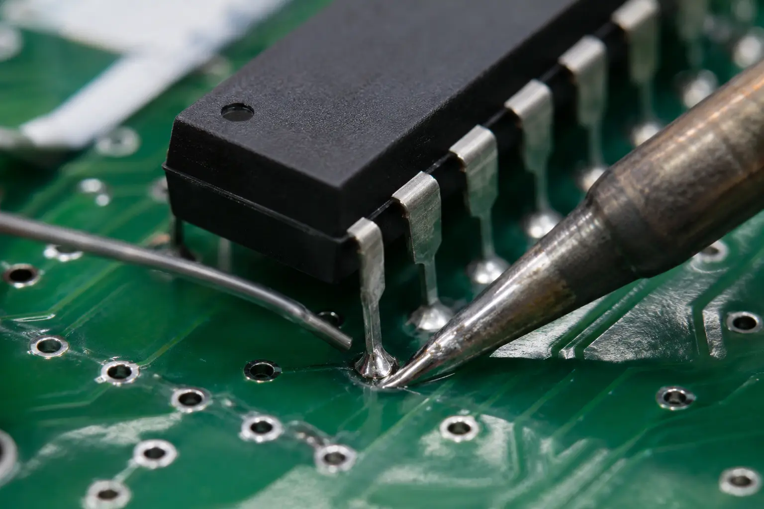
Correctly installing a dual in-line package ensures stable electrical connections and reliability for years of service:
Soldering Steps:
- Place the DIP package with two rows of pins into the PCB holes, aligning the notch in the package with the Pin 1 indicator.
- For precision, use a DIP socket if possible; this prevents heat damage from direct soldering and allows for easy replacement.
- Solder each pin individually, ensuring thorough wetting of both pin and pad. Too much solder can create bridges between pins, while too little may cause poor connections.
- Inspect under magnification; use a solder sucker or wick to clean up excess solder if necessary.
Socketing Benefits: DIP sockets make replacement and debugging simple—they’re especially useful when prototyping or when the IC may be programmed externally.
Installing DIP Tips:
- Straighten all pins before attempting to insert the component package.
- On double-sided or plated-through PCBs, be extra careful with soldering heat.
- For legacy systems, gently pry out old DIP ICs with a DIP extractor tool rather than bare hands to avoid damaging the PCB or adjacent electronic components.
Benefits of Using DIP Packages
DIP packages remain a top choice for education, prototyping, and repair—here’s why:
- Rapid prototyping: Drop into breadboards with perfect pin spacing.
- Easy replacement: Inserted into a socket or desoldered/replaced by hand.
- Durable and reusable: The package body protects against moderate heat, and robust two rows of pins stand up to regular handling.
- Excellent for learning: The 2.54mm pin spacing and clear row of pins provide tactile feedback and visible orientation—ideal for training.
- Cross-compatibility: Pin count and physical standards are so widely adopted that DIPs remain available for most common logic, memory, and analog ICs.
List of Example Use-Cases:
- Building or repairing vintage electronic devices.
- Modern DIY kits (e.g., Arduino boards using DIP microcontrollers).
- Quick replacement of failed ics in consumer electronics.
- Education labs teaching soldering and circuit design.
- Prototyping new products on breadboards or perfboards.
DIP LED and DIP switches: Widely available in DIP format—DIP switches are classic for configuration settings, while DIP LED packages are prized for reliability in signaling circuits.
Limitations and Challenges
Despite their versatility, DIP packages do face several limitations—especially in today’s densely packed, miniaturized PCBs:
- Board space: DIP packages are larger than soic packages and other SMT solutions, taking up more room on a circuit board.
- Pin count limits: The number of pins is capped around 64; devices with higher I/O counts require more advanced package types or surface-mount solutions.
- High-speed constraints: Long leads in a DIP can introduce signal noise, making SMT and QFP/QFN packages better for RF and high-speed logic circuitry.
- Manual assembly: DIP ics must usually be inserted and soldered by hand or by wave soldering machines; they are not readily compatible with automated surface-mount assembly.
- Obsolescence: Some new ICs are not available in DIP packages at all; adapters may be needed for prototyping.
When not to use DIP packages: If your design requires the smallest possible product footprint, or is going into high-volume, automated production, SMT and small outline package (SOP package) options are usually more efficient.
Popular DIP ICs and Their Functions
Available in DIP: A huge variety of ICs are available in DIP and remain staples for modern and legacy applications.
| IC Category | DIP Example(s) | Pin Count | Typical Function |
| Timer/Analog | 555 Timer, LM358 | 8 | Oscillator/amplifier |
| Logic Gates | 7400, 4011, 74HC595 | 14–16 | NAND/AND, shift register |
| Microcontroller | ATmega328P, PIC16F | 28–40 | Embedded computing |
| EPROM/EEPROM | 27C512, 28C256 | 28 | Reprogrammable memory |
| CPU | Z80, 6502 | 40 | Vintage computing/controls |
| Op-amps | LM741, LM324 | 8/14 | Signal amplification |
| RS-232 Interface | MAX232 | 16 | Serial communication |
| DIP LED Array | HDSP-0760 | 16–24 | Visual display |
| DIP Switches | N/A | Varies | User-configurable settings |
DIP Package in Electronic Devices & Applications
DIP packages have earned their place in many types of electronic devices:
- Used in consumer electronics: DIP ICs are common in everything from synthesizers to alarm panels and test gear, due to their durability and pin compatibility.
- Repair & Maintenance: For legacy devices, being available in dip format makes fixes possible without major redesign.
- Specialized & Industrial Controls: Some high-reliability ceramics (ceramic dip/ceramic dual in-line package) are still in use for military and aerospace.
- Educational Kits: The pin count and tactile size of the DIP package make it ideal for hands-on circuit board training and STEM kits.
DIP vs Other Package Types: SOIC, SMT, and SOP
DIP vs SOIC packages:
- SOIC stands for Small Outline Integrated Circuit, a surface mount (SMT) form. The soic package offers a much smaller footprint for high-density PCBs but sacrifices hand-solderability and breadboarding.
- DIP, on the other hand, is ideal for through-hole mounting and can be easily inserted and replaced in a dip socket.
- DIP vs SMT: The main difference is mounting method (through-hole vs. SMT), size, and suitability for prototyping.
DIP vs SOP package:
- SOP is also a small outline package, widely used in modern SMT designs, offering shorter pin leads, less parasitic capacitance/inductance, and efficient use of PCB space.
| Feature | DIP/Through-Hole | SOIC/SOP/SMT |
| Installation | Manually in PCB holes | SMT reflow machines |
| Pin Spacing | 2.54mm | 1.27mm or less |
| Pin Count | Up to 64 | Up to 200+ |
| Prototype use | Yes, easy | Not suited for breadboards |
| Repairability | High, because socketable | Low, requires SMD tools |
| Package body | Rectangular, bulkier | Low profile, compact |
DIP vs QFP/QFN/BGA: High IO count and ultracompact modern applications use quad flat packages or ball grid arrays—usually impossible to hand assemble or prototype without specialized gear.
Evolution from DIP to SMT and Modern Trends
The evolution from DIP packages to SMT was driven by the ever-shrinking size of electronic devices, the need for more automatic assembly, better electrical performance, and lower cost per component package at scale.
- Early designs featured the DIP package size as a constraint; modern designs aim for minimal profile and maximal functionality.
- SMT (Surface Mount Technology) enables shorter signal paths, higher speeds, and double-sided PCB assembly.
- Still, certain ICs—like microcontrollers and analog chips—are often available in dip packages for prototype and small-batch production.
Industry trend: Most new ICs are available only in SMT. However, many classic ics are still available in DIP format for backward compatibility and education. Adaptors let designers use SMT chips on breadboards with DIP headers for testing.
Expert Tips and Best Practices
Maximize your DIP experience with the following professional tips:
- Always use anti-static handling: ICs are sensitive to ESD; store in antistatic tubes/foam.
- Align DIP pins carefully: Misaligned pins can damage the socket or PCB holes.
- Use a dip socket for valuable or programmable ICs: This decreases stress on both PCB and component when removing or swapping chips.
- Test circuits on a breadboard first: Prototypes using DIP packages let you test before committing to a final printed circuit board.
- Double-check pin orientation: The notch or dot shows which side of the dip is Pin 1.
- For heavy use or harsh environments: Consider ceramic DIP and proper conformal coating.
- For rare or obsolete parts: Buy from reputable suppliers; avoid re-marked or counterfeit chips by checking markings and package design features.
- When upgrading legacy designs: Match pin count, spacing, and package body size precisely to avoid costly mistakes.
Buying and Identifying DIP Packages
How to select the right DIP:
- Review the pin count, package width, and row spacing needed for your board.
- Consult supplier catalogs for available in dip parts; common logic, memory, microcontroller, and analog ICs are always stocked in DIP versions.
- For ceramics (ceramic package), scrutinize markings to avoid aged or fake parts—CDIP is common in aerospace and defense, but only from reliable vendors.
- Always match not just function, but also component package, pinout, and electrical ratings.
Authenticity and sourcing:
- Use trusted vendors for ICs and other electronic component package types.
- For discontinued DIPs, reputable surplus dealers may have stocks, but beware package re-marking—a common fraud.
FAQs
Q: What defines the “dip package” compared to other packages?
A: The DIP package is a rectangular body IC package with two parallel rows of pins, intended for through-hole soldering or socketing into a PCB. Major benefits include mechanical strength, easy hand soldering, and broad compatibility with breadboards and sockets.
Q: How do I identify the right orientation for a dual inline package?
A: Always look for the notch or dot on the top of the package body; Pin 1 is immediately to the left of this marking when viewing from above.
Q: Can I convert a DIP IC to surface-mount for modern PCBs?
A: DIP adapters allow you to use DIP chips on SMT boards, but the reverse—using soic or smt-only devices in a DIP socket—usually requires a dedicated breakout board.
Q: Are DIP packages obsolete for new electronic component design?
A: While not common for ultra-dense/high-speed applications, DIP packages remain vital in rapid prototyping, education, field service, and legacy system maintenance.
Q: Are DIP components available today?
A: Yes, many microcontrollers, logic ICs, analog chips, and specialty parts are still available in DIP format.
Conclusion: Should You Use DIP in Your Designs?
DIP packages have outlasted most other electronic component package types thanks to their balance of durability, accessibility, and mechanical simplicity. If your project values easy repair, prototyping, or field service—and space isn’t at an absolute premium—choosing or using dip packages is often the smart move. For high-density, high-speed, or mass-manufactured designs, move to SOP, SOIC, or QFP as needed.
In educational labs, prototyping teams, and vintage repairs, the dip package remains standard. For the foreseeable future, DIP is likely to stay available in dip and an important part of the electronics toolkit.