Introduction
In the ever-evolving PCB industry, the smallest design details can greatly impact the success, reliability, and yield of your printed circuit board. One such detail is the humble fiducial mark. These tiny reference points are essential for both high-volume PCB manufacturing and rapid prototyping, ensuring precise alignment and accurate component placement across a vast range of applications.
This comprehensive guide to PCB fiducials will explain what fiducial marks are, why they are fundamental to the assembly process, how to place fiducials, and the standards you need to follow so that your board production runs smoothly every time. We’ll cover the types of fiducial markers, common errors in fiducial placement, and advanced tips for panelization, rigid-flex circuits, and IPC Class 3/mission-critical products.
Whether you’re a new PCB designer or an industry veteran seeking best practices, this is your one-stop guide to fiducials in PCB—complete with actionable insights drawn from real-world manufacturing.
What is a Fiducial Mark and Why Is It Essential in PCB Design?
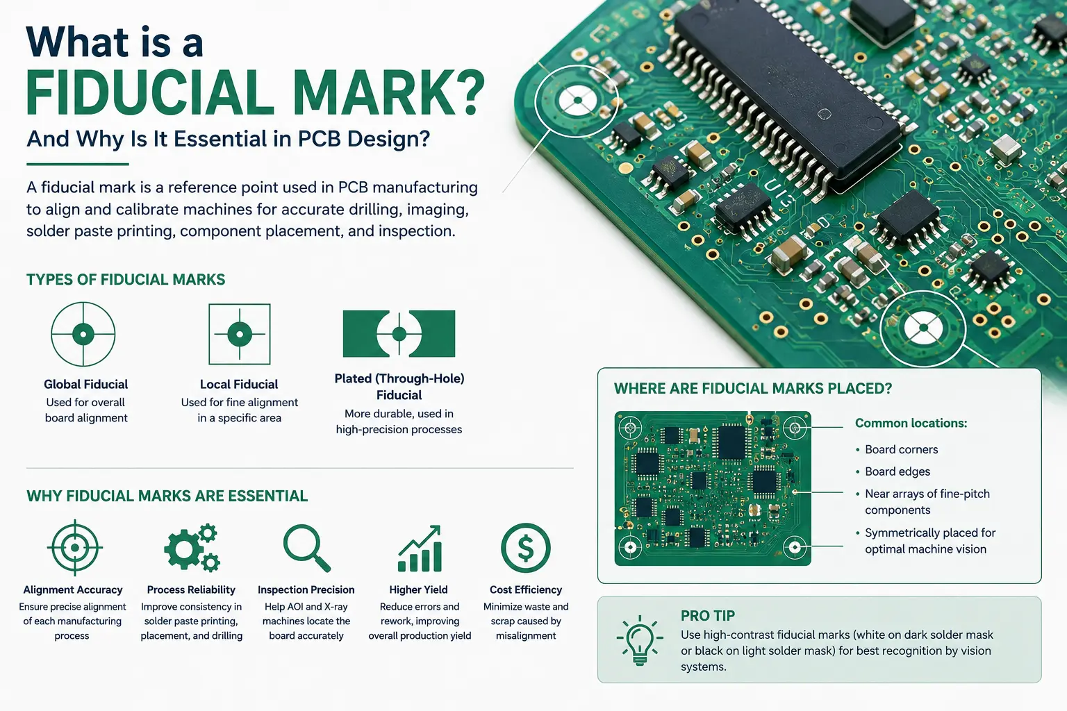
A fiducial mark is a clearly defined, optically recognizable reference point on a PCB board. The primary function of fiducials is to act as alignment marks for automated assembly machines—most notably pick-and-place equipment and inspection systems. Fiducials are almost always solid circular copper pads (1–3 mm diameter), free of solder mask or silkscreen, with a generous clearance to other features.
Why use fiducials? In SMT systems, machine vision algorithms detect these landmarks to map between the CAD file’s digital reference and the physical placement or inspection of the actual board during the assembly process. Without fiducials, registration errors, component misplacement, and yield loss are inevitable in production.
The importance of fiducial marks cannot be overstated in modern pcb design. As the density of PCBs rises, with BGAs, fine-pitch QFNs, and high-pin-count devices, even a 50 μm shift can lead to open or bridged joints. Fiducial markers are essential in maintaining correct orientation of the entire PCB, correction for rotation of the PCB, and X/Y board position.
Key points about fiducial marks in PCB assembly:
- Serve as a universal reference point for PCB alignment.
- Used by every automated alignment system on the assembly line.
- Necessary for precise component placement accuracy—especially for fine-pitch SMT components.
- Must get fiducial markers right for high first-pass yield and reliability.
A properly specified fiducial marker must maintain both its geometry and position throughout the entire assembly process.
Types of Fiducial Marks and Their Placement
The types of fiducial marks on a PCB can largely be separated into global fiducials and local fiducials. Both serve critical roles in ensuring accurate alignment marks for a flawless pcb assembly.
Global Fiducials
Global fiducial marks—sometimes called panel fiducials—are placed at the corners of the PCB or on panel rails in multi-board panelization. Three global fiducials (typically in an L-shape) are recommended for high-reliability systems, while two global fiducial marks are the bare minimum. Their primary purpose is to tell the vision system the board’s position and orientation, allowing for correction of translation, rotation, and slight stretch or skew (nonlinear distortion).
Where are global fiducials positioned?
- At least 5 mm from any PCB edge or V-score/tab route.
- Placed at two or three well-separated board corners. This 3-point system supports affine (planar) transformation correction.
- Must have clear solder mask relief (at least 0.5 mm, often more).
Global Fiducial Location
| Global Fiducial Points | Board Location | Correction Ability |
| Two global fiducials | Opposite corners of the pcb | X/Y translation, rotation |
| Three global fiducials | L-shape at corners of the pcb or panel rails | Full planar/affine |
Local Fiducials
Local fiducials are smaller alignment marks situated near critical or high-density components, such as BGA, QFP, or QFN packages. Local fiducials near these devices help correct local board stretch, twist, or warpage that global marks can’t resolve.
Use local fiducials if:
- You have components with pitch ≤0.5 mm (e.g., BGA, QFN, QFP).
- Specific high-density or high-value parts require extra accuracy.
- The PCB fab recommends them for challenging flexible, rigid-flex, or large-format boards.
Panel Fiducials and Special Panelization Practices
When multiple PCBs are fabricated and assembled together on a panel, panel fiducials—large fiducials on the panel rails—provide a master alignment reference for the entire PCB array. Additionally, each sub-board can have its own global/local fiducials for further accuracy and downstream inspection.
Global fiducials on the panel rails anchor the entire assembly process.
How Fiducial Markers Guarantee Precision in PCB Assembly
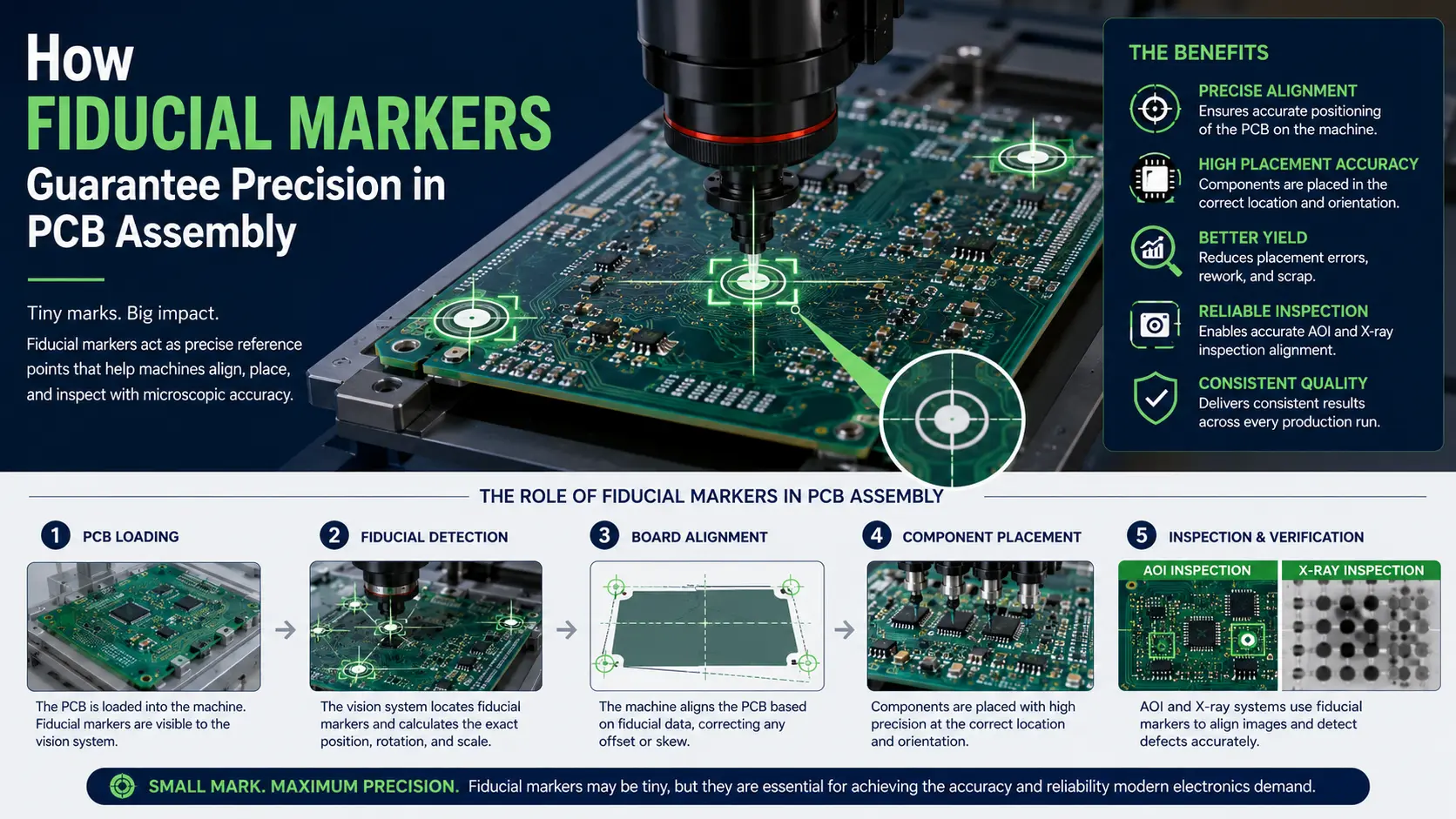
How do fiducials work? Every step of the pcb manufacturing and SMT process depends on fiducial marks for alignment of the physical and digital domains. The assembly line’s vision system locates fiducials and recalculates the affine transformation (translation, rotation, scaling) needed to map from CAD coordinates to actual PCB coordinates.
Key assembly steps using PCB fiducials:
- Stencil printing: The stencil aligns with global panel fiducials, so solder paste lands perfectly on copper pads.
- Pick-and-place machines during PCB assembly: Systems find the fiducials, orient the board, and place each SMT component at the correct location based on the transformed file coordinates.
- AOI/SPI inspection: AOI cameras register the PCB orientation and mapping using fiducial markers, so defects are accurately assigned to the correct area.
- Panelization and depaneling: Panel fiducials on the rails ensure the entire PCB array stays registered throughout processing and separation.
- Testing and traceability: Boards with well-documented fiducial marker placement are easier to track, debug, and rework when issues do arise.
Fiducial Design Guidelines for PCB Manufacturing
Designers must get fiducial markers right—not only for assembly, but for board fabrication, stencil manufacture, and inspection. Here’s your cheat sheet for fiducial design in the real world:
Physical and Geometric Standards
| Aspect | Recommendation | Notes |
| Shape | Solid filled circle | Do not use ovals, squares, or crosses |
| Fiducial diameter | 1–3 mm (2 mm typical) | Consistency within ±25 μm (Class 3) |
| Solder mask | None: Clearance diameter 0.5–1 mm larger than pad | Ensures strong optical contrast |
| Keepout | ≥0.5–1 mm clearance to all copper, no silkscreen | Reduces false positive detection |
| Edge clearance | ≥5 mm from edge, clamp, or break line (tab/V-score) | Avoids panel/mechanical interference |
Fiducial Placement and PCB Layout Techniques
The placement of fiducial marks should never be an afterthought in your pcb layout. Fiducials must be placed on all critical boards, visible on every layer that sees automated assembly, and included in every design sent for manufacturing and assembly. Use fiducial markers in your design responsibly—start all layouts by planning fiducials on the board.
General Rules for Fiducial Placement:
- Place at least two global fiducial marks on opposite corners or—as best practice—three global fiducials in a non-linear (L-pattern or triangle) arrangement for distortion compensation.
- When you add fiducials, ensure the fiducial diameter and clearance area are the same across the entire PCB.
- Local fiducials should be placed near fine-pitch parts; two local fiducials at opposite corners of a BGA are encouraged.
- Never place fiducials too close to edges, edge connectors, V-scores, or panel routes; fiducials on the panel rails should always avoid intrusion into breakaway areas.
Using Fiducial Markers in PCB Design Software
Most modern pcb design software (such as Altium Designer, KiCAD, OrCAD, Eagle, and others) have defined tools or templates for placing fiducial markers in PCB layout, specifying pad size, solder mask opening, and keepout zone. Before export, always perform a Gerber review to ensure the fiducial is fully exposed, with no mask or silkscreen encroachment.
Checklist:
- Are there three global fiducial points, well-separated on the PCB panel?
- Do local fiducials exist on every BGA, QFN, or ultra-fine-pitch site?
- Is every fiducial a filled circle, with no nearby copper or reference text?
- Is the clearance from V-scoring or routing at least 5 mm?
- Does your design documentation (FAB notes, README, assembly drawing) clearly label every fiducial marker?
Advanced Fiducial Strategies: Panelization, Flex PCBs, and High-Reliability Assembly
Panelization and Fiducials on the Panel
When it comes to pcb assembly of panelized boards, panel fiducials and board-level fiducials each play unique roles. Fiducials on the rails of the panel (outside the active board area) provide the macro-alignment for SMT stencil and pick-and-place equipment. Each sub-board should have its own global fiducials if it will be separated and tested individually.
Tip: For complex panels, always coordinate with your assembler to find the fiducials that their process requires for registration and rotation of the PCB.
Rigid, Flexible, and Rigid-Flex Circuits
Flexible PCBs and rigid-flex circuits have unique challenges—material shrinkage, stretching, and planar warping can cause unpredictable positional errors. Here, designers use global fiducials across both rigid and flex regions, and sometimes add extra “bowtie” or tie-in copper features adjacent to all critical flex-to-rigid transitions for improved alignment.
In high-reliability environments such as medical or aerospace, the fiducial marker must maintain Class 3 IPC tolerances, with every aspect of fiducial placement and finish clearly documented in the production package.
Common Fiducial Mistakes and Professional Solutions
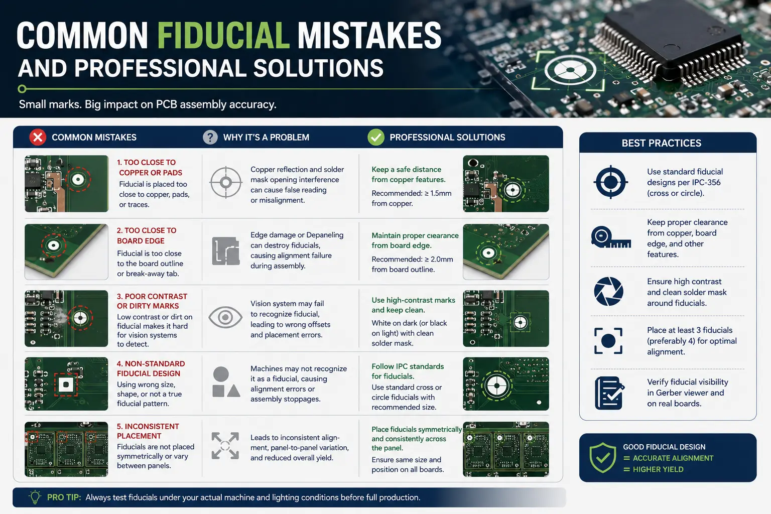
Errors in Fiducial Placement: What to Watch For
Even experienced PCB designers sometimes make the following mistakes:
- Placing fiducials too close to board edges(risking loss during depaneling or clamp interference)
- Non-circular or inconsistent fiducials(confusing vision systems)
- Overlapping solder mask or silkscreen(blocks optical detection)
- Using drilled holes or nonstandard shapes(these do not substitute for standard fiducials)
- Missing local fiducials near BGAs(the most common reason for placement errors in high-speed assembly lines)
- Excessive redundant fiducials(vision systems may “see” the wrong one)
Professional Solutions
- Always run a dedicated DFM review specifically for fiducials in both fabrication and assembly checklists.
- Communicate with both your PCB manufacturer and assembly house; provide versions of the board with clearly labeled fiducials.
- Use standard fiducial design libraries or templates in your EDA tool.
- After Gerber export, visually inspect every layer to check for accidental mask or silkscreen overlap.
- For mass production, request a “first-article” build to validate fiducials in PCB assembly, including automated optical inspection.
Conclusion, Actionable Takeaways, and Further Resources
Key Takeaways
- Fiducials are positioned strategically for every phase of PCB manufacturing and assembly. Poor fiducial design cripples the entire PCB assembly process.
- Use at least two global fiducials, but three global fiducial markers are strongly recommended for rotation, PCB orientation correction, and distortion compensation.
- Local fiducials near high-density and fine-pitch components (BGA, QFN, QFP) are a must for advanced, high-yield SMT lines.
- Keep all fiducials on the board clear of solder mask, copper, silkscreen, and edge features.
- When panelizing, global fiducials on the panel rails are required; sub-boards should have their own marks if assembled/tested apart.
- Use global fiducials for the master reference; local fiducials for pinpoint accuracy around sensitive ICs.
- Ensure all PCB fiducial markers are verified via both visual and automated DFM checks.
- Placing fiducial markers right is essential for industry compliance and yield.
Pro Tips
- Mark every fiducial in your README or documentation—global, local, and panel—so manufacturers can easily find the fiducials and follow the intended use of fiducial.
- If unsure, always over-communicate with your assembly partner about alignment and fiducial requirements.
- For new processes (HDI, ultra-fine pitch, flex/rigid-flex) or high-reliability, run a dedicated fiducial DFM panel before scaling up.
FAQ: Fiducials and Fiducial Marks in PCB Assembly
-
What is a fiducial on a PCB?
A PCB fiducial is a small reference mark, usually an exposed circular copper pad, used by automated assembly equipment to identify the board’s exact position and orientation.
-
What is the purpose of a fiducial marker on a PCB?
Fiducial markers help pick-and-place and inspection systems correct positioning errors before components are placed or inspected, improving SMT assembly accuracy.
-
How many fiducials do you need on a PCB?
Three global fiducials are commonly recommended for accurate X-Y positioning and rotational correction. Some designs may also use local fiducials near fine-pitch components.
-
Where should a fiducial marker be placed on a PCB?
Global fiducials are typically placed near the corners of the PCB and spaced as far apart as practical. They should remain clear of components, traces, silkscreen, and other visual features.
-
What are PCB fiducial markers made of?
PCB fiducials are usually exposed copper pads with a consistent surface finish such as ENIG or bare copper, surrounded by a solder-mask clearance area.
-
What are the different types of fiducial markers on a PCB?
The main types are global fiducials, which reference the entire PCB or panel, and local fiducials, which provide additional alignment around high-precision components.
-
Are fiducials required on every PCB?
Not always. Simple boards may be assembled without dedicated fiducials, but they are strongly recommended for automated SMT assembly, especially for fine-pitch and high-density designs.
-
Can PCB fiducial markers be removed?
They can be omitted if the assembly process does not require them, but removing fiducials from an SMT design may reduce placement and inspection accuracy.
-
Do fiducial markers remain on the PCB after assembly?
Yes. PCB fiducials normally remain as permanent features on the finished board and do not affect its electrical function.
-
Why are fiducials important in PCB layout?
Properly designed fiducials give automated equipment reliable visual reference points, helping reduce component placement offsets, rotation errors, and alignment problems during PCB assembly.