The rapid advancement in modern electronics demands packages that are compact and offer high connection density. Ball Grid Array (BGA) technology is the exact solution manufacturers need for modern PCB designs.
BGA chips are becoming the first choice in processors, memory modules, graphics devices, and miniature embedded systems. This comprehensive guide on Ball Grid Array chips covers the basics, internal structure, operating principle, applications, challenges, and more.
What is a BGA Chip?
A Ball Grid Array chip (BGA chip) is a type of surface-mount packaging for integrated circuits that uses a grid of solder balls on the chip’s underside instead of traditional pins to create electrical connections with the PCB.
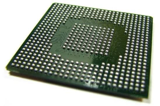
Traditional leaded packages like Quad Flat Package (QFP) rely on delicate metal leads running along the component’s edges. BGA packaging takes a different approach. It spreads connections over the entire underside of the chip. This layout offers higher pin counts in a smaller footprint, along with stronger electrical performance and more efficient heat transfer.
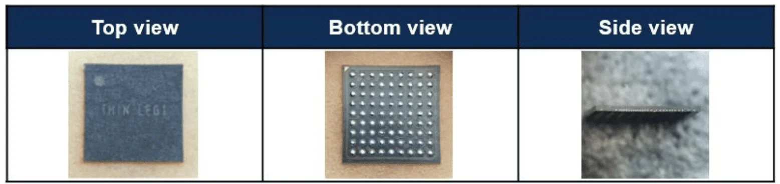
BGA packages are now widely used for mounting complex components such as GPUs, CPUs, FPGAs, and memory chips onto PCBs in laptops, embedded systems, smartphones, and networking equipment. BGA technology is finding applications everywhere where older package types can’t keep pace with modern performance and space requirements.
What’s Inside a BGA Chip Package?
The working principle of a BGA chip package will only become clear if you first understand its internal structure.
The internal composition of a BGA package comprises many engineered layers working together to link the tiny silicon die to the PCB below. All this happens while managing electrical flow and heat dissipation, as well as physical durability. Let’s uncover each layer to see what’s inside the BGA assembly:
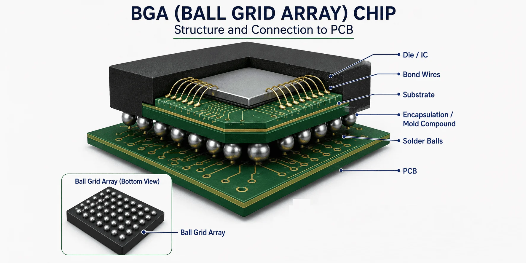
Semiconductor Die
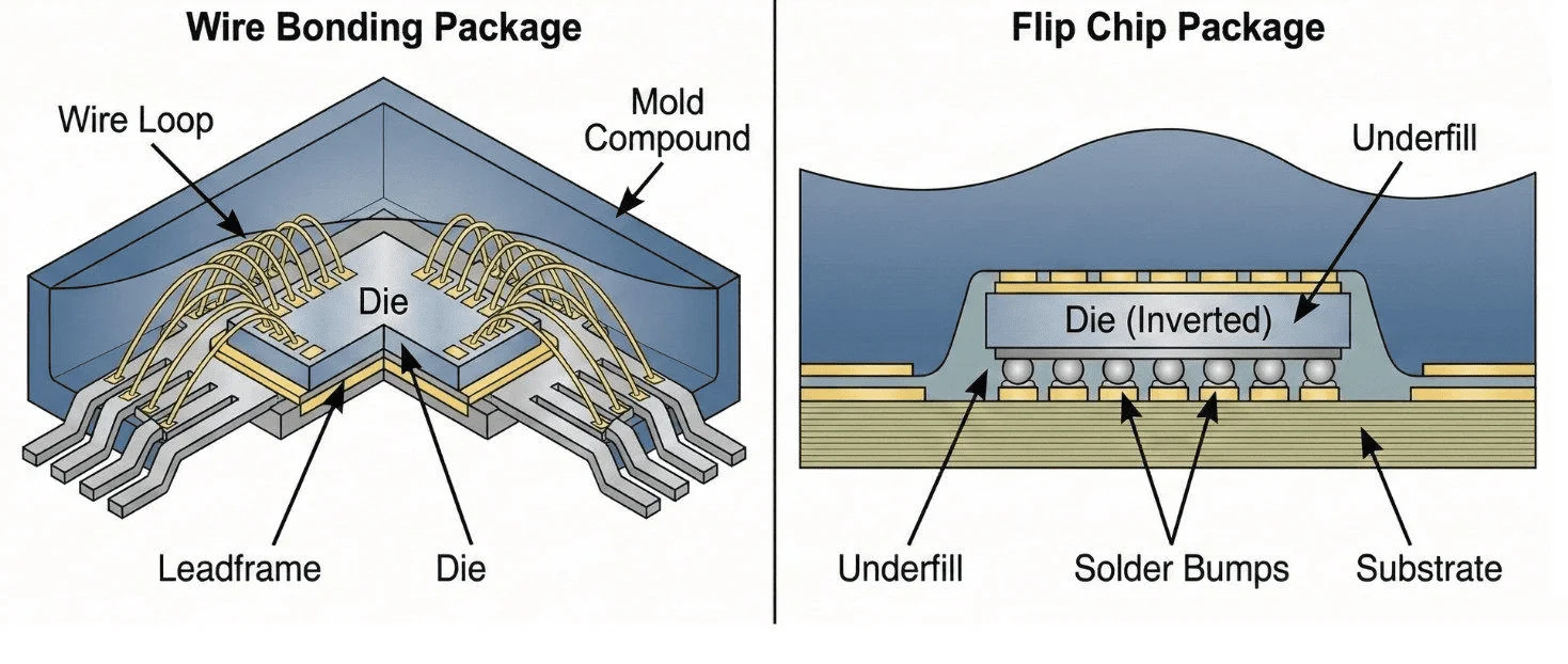
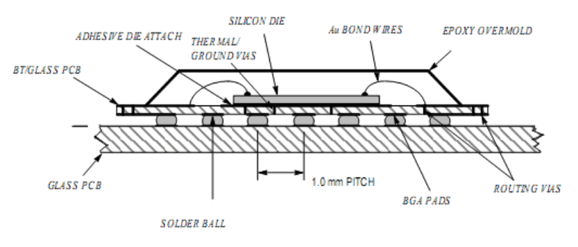
As an active silicon component, it is where all the actual computing and signal handling takes place. It’s also where most of the heat originates during operation. In wire-bonded designs, this die is bonded to the substrate below using either Die Attach Film (DAF) or a conductive epoxy adhesive.
Interconnection Layer (Wire Bond / Flip-Chip)
This layer gets the most attention from packaging engineers because it’s the link between die and substrate. Older, more conventional BGA builds use wire bonding, which involves extremely thin gold or copper wires connecting the pads around the die’s edge to the substrate underneath.
Newer high-performance chips flip the die and mount it face-down onto the substrate through tiny solder bumps in a process called flip-chip bonding. This shortens the electrical path and reduces inductance.
Package Substrate
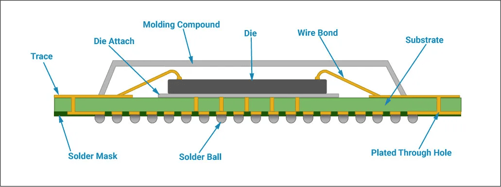
The substrate is like a compact PCB living inside the chip, which is built from layered organic or ceramic material. Its job is redistribution. It takes the tightly packed connections coming off the die and spreads them out to align with the wider spacing of the solder balls below.
Higher-end substrates use laser-drilled microvias to move signals from top to bottom without loss. Built into the substrate are also dedicated power and ground planes to keep power delivery to the die stable.
Solder Ball Array
At the base of the BGA package is the array of solder spheres that will bond to the main circuit board. Two things matter here:
- Ball pitch: The spacing between individual balls, somewhere between 0.4mm and 1.0mm.
- The solder material: Often a lead-free alloy like SAC305.
Engineers need to carefully choose them to ensure the connections hold up mechanically and electrically over time after reflow soldering. These solder balls also create physical clearance between the BGA chip and the board, which helps absorb stress and resist fatigue from temperature swings.
Encapsulation and Underfill
The die and its wire connections are fragile, so the top of the BGA package gets sealed with a hardened epoxy mold compound to guard against moisture, oxidation, and physical impact.
Flip-chip packages (FCBGA) take this a step further with underfill, which is an epoxy injected into the narrow space between die and substrate. This underfill helps spread out thermal stress and keeps the micro-bumps from cracking under repeated heating and cooling cycles.
The Working Principle of a Ball Grid Array Package
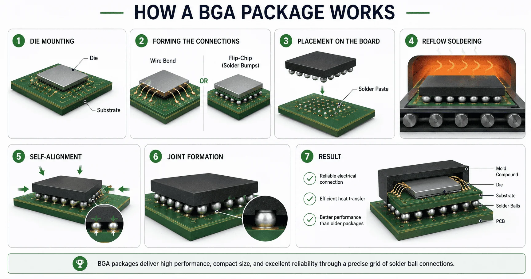
A BGA package links a chip to its circuit board through a grid of solder spheres lining its underside. This gives each ball a matching pad on the PCB below. Let’s understand how that connection actually comes together step by step during BGA PCB assembly:
- Die Mounting: The silicon die is fixed onto a multilayer substrate, which acts as the internal wiring network for signals and power.
- Forming the Connections: The die links to that substrate through either fine wire bonds or flip-chip solder bumps. The choice depends on how much performance the chip needs.
- Placement on the Board: The finished package is set onto PCB pads that have already been coated with solder paste.
- Reflow Soldering: The BGA assembly passes through a reflow oven, where controlled heat melts the solder.
- Self-Alignment: As the solder liquefies, surface tension pulls the package into precise alignment with the pads automatically.
- Joint Formation: After cooling, the melted solder solidifies into joints that handle electrical conductivity and heat transfer all at once.
The result is a connection method that beats older leaded packages and offers tighter signal paths with lower parasitic inductance and better heat management.
Types of BGA Packages
Not every BGA package is identical. The substrate material and chip orientation all change based on what the application demands, such as thermal load, speed, size constraints, or cost.
The following are different types of BGA packages commonly used:
PBGA (Plastic Ball Grid Array)
PBGA is the most widely used BGA chip type in consumer electronics, microcontrollers, memory chips, and others. It’s built on a BT resin substrate, sealed with OMPAC or GTPAC technology, and rated JEDEC Level 3 for reliability. Ball counts usually range from 200 to 500. It offers a solid mix of low cost and dependable performance, though thermal handling is only moderate.
CBGA (Ceramic Ball Grid Array)
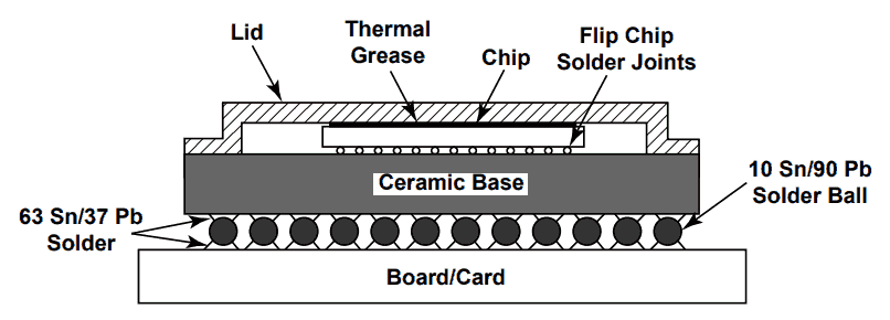
CBGA is the go-to for high-heat environments, such as aerospace and telecom. Its 10:90 tin-to-lead ratio and high melting point mean it needs the C4 (Controlled Collapse Chip Connection) method for bonding to the board. It costs more than PBGA but delivers far better thermal conductivity and electrical insulation.
TBGA (Tape Ball Grid Array)
TBGA uses a flexible polyimide tape substrate, which keeps the package thin. That characteristic and strong heat dissipation make it suited to slim laptops and compact high-performance devices. Wire bonding is used for face-up chips, while flip-chip handles face-down configurations.
EBGA (Enhanced Ball Grid Array)
EBGA builds on the standard PBGA design by adding dedicated heat-sink capability. A dam structure is formed around the chip on the substrate, and a liquid sealing compound fills it in to lock the component down. Chips in this configuration face downward, with wire bonding handling the connection between chip and board.
FCBGA (Flip Chip Ball Grid Array)
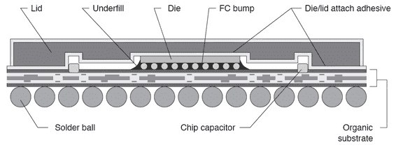
FCBGA flips the die face-down and attaches it directly to the substrate via micro-bumps. This shortens the electrical path and cuts inductance and delay. This makes it the standard choice for high-speed CPUs/GPUs and networking chips. It uses BT resin (63:37 tin-to-lead) instead of ceramic, so the cost is lower while allowing the chip to self-align without special equipment.
Figure 10. Flip Chip Ball Grid Array (FCBGA) cross-sectional view. Source PCB HERO
MBGA (Metal Ball Grid Array)
MBGA uses a metal-ceramic substrate with circuitry formed via sputtering. Chips face down and connect through wire bonding. The metal base gives it strong electrical performance and good heat dissipation.
Micro BGA
Micro BGA uses a packaging-tape substrate with the chip mounted face-down, separated by an elastomer layer that absorbs thermal expansion stress. Its main strength is size, so it enables compact and high-density designs in memory products while keeping pin counts low.
Advantages of Using a BGA Chip
BGA packaging brings more than just a smaller footprint. It delivers real gains in electrical performance and manufacturing efficiency. The main advantages of using a BGA chip include:
- High I/O Density: Using the full underside of the chip instead of just its edges lets BGA pack in hundreds or thousands of connections within a much smaller area than a comparable leaded package.
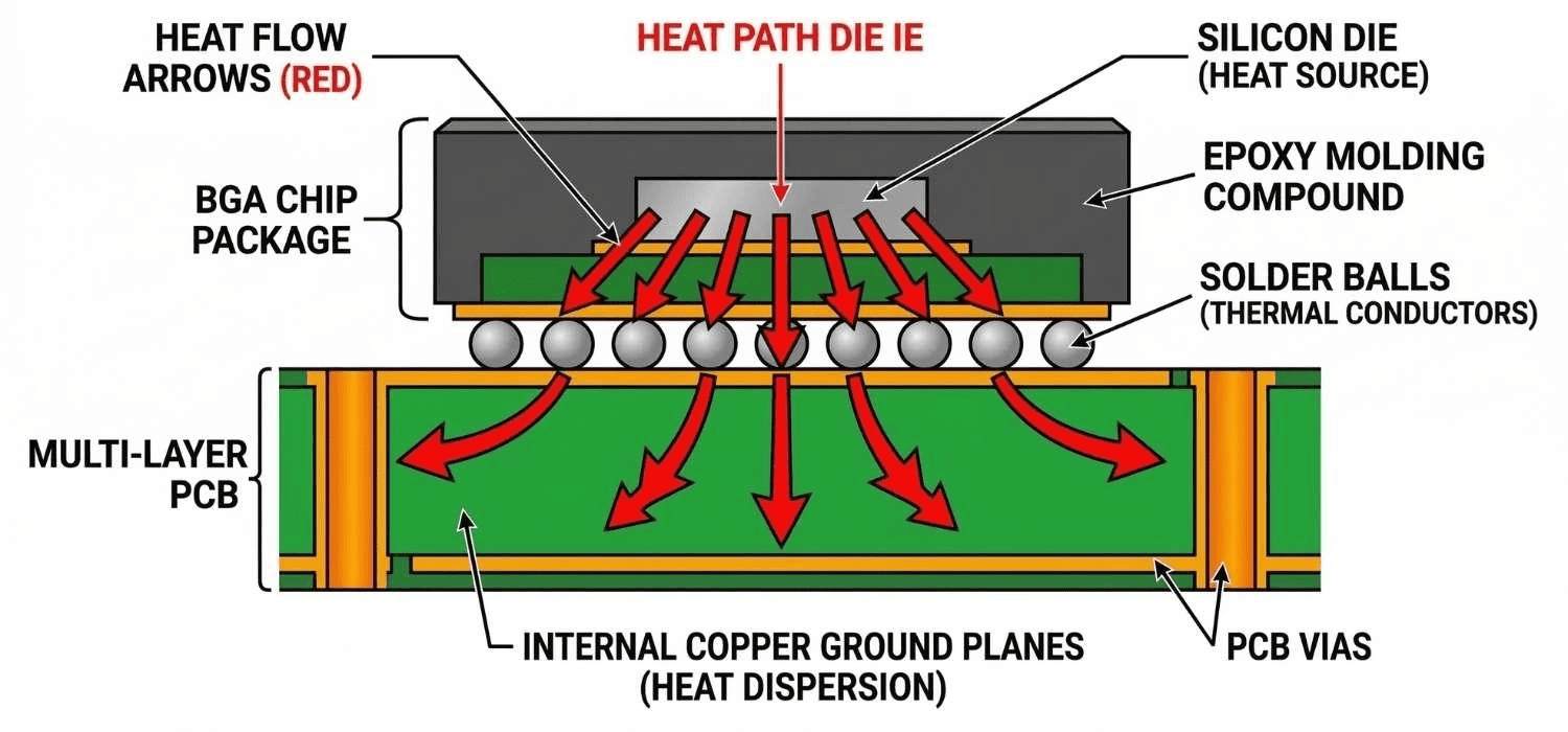
- Better Heat Management: Heat from the die travels directly down through the solder balls into the PCB’s copper layers. This makes the board itself act as a heat sink and keep hotspots to a minimum.
- Stronger Electrical Performance: Shorter connection paths mean lower parasitic inductance and resistance, which translates to cleaner signal transmission at high speeds and frequencies.
- Self-Aligning During Assembly: Molten solder’s surface tension naturally pulls a misplaced chip back into the correct position, which reduces placement errors during reflow.
- Compact, Space-Saving Design: Replacing external leads with solder balls under the chip lets designers fit more functionality into thinner and smaller devices.
- Easier Rework: Larger solder pads make desoldering and repair simpler. This helps cut down on downtime and repair costs.
- Improved Mechanical Reliability: Solder ball joints resist the fatigue that lead connections suffer from repeated thermal cycling. This gives BGA chips a longer usable lifespan.
- Built for Automated Assembly: The flat top and grid layout of BGA packages make them easy to place precisely using pick-and-place machines, which speeds up high-volume production.
These advantages highlight why BGA chips are becoming the standard packaging choice in smartphones and high-performance computing hardware.
Challenges/Limitations of BGA Chips
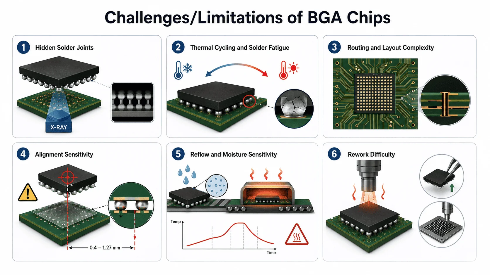
BGA chips solve many problems, but they also introduce a fresh set of engineering hurdles during design and assembly. Some of the main challenges/limitations are:
Hidden Solder Joints
Because every connection sits underneath the package, there’s no way to visually check for poor wetting or misalignment. Manufacturers have to rely on X-ray inspection, which adds cost and complexity to quality control.
Thermal Cycling and Solder Fatigue
The BGA chip and PCB expand and contract at different rates as temperatures shift. This mismatch is known as CTE (Coefficient of Thermal Expansion) mismatch. Repeated over thousands of heating and cooling cycles, this stress builds up around the outer solder balls and can cause them to crack.
Routing and Layout Complexity
Getting traces out from under a dense, high-pin BGA package isn’t simple. It requires HDI (High-Density Interconnect) techniques, involving extra board layers, fine trace widths, and laser-drilled microvias.
Alignment Sensitivity
With ball pitches as tight as 0.4–1.27mm, so just a fraction of a millimeter of misplacement during assembly can result in shorts or open connections. Pick-and-place equipment needs to hold very tight placement tolerances to avoid defects.
Reflow and Moisture Sensitivity
BGA chips need a controlled reflow profile. Uneven heating can leave joints weak or incompletely melted. It can also shift the package out of position. Some BGA packages also absorb ambient moisture over time, which can expand during reflow and damage the part if it isn’t baked out beforehand.
Rework Difficulty
Since joints are hidden and inaccessible, repairing/replacing a BGA chip requires specialized equipment like hot-air rework stations and reballing kits. In addition, there is a need for precise temperature control to avoid damaging neighboring components.
Applications of BGA Chips
BGA chips have become a default choice in almost every category of modern electronics due to their high pin density and compact size. Some of the main applications of BGA chips are:
High-Performance Computing
CPUs, GPUs, FPGAs, and ASICs rely on BGA packaging to manage large I/O counts and deliver power efficiently. The short interconnect paths also help minimize signal distortion, which matters for general-purpose and high-performance servers.
Mobile and Consumer Electronics
Smartphones, tablets, laptops, wearables, and gaming consoles all lean on fine-pitch BGA packages to squeeze more functionality into limited board space. Processors and memory chips in these devices depend on BGAs’ compact footprint to hit tight size and performance targets.
Networking and Telecommunications
Routers, switches, and base-station equipment use BGA chips to handle multi-gigabit data transfer and manage the heat that comes with it. The electrical characteristics of FCBGA make it well-suited to high-speed data infrastructure.
Automotive and Industrial Systems
Electronic/industrial control units and infotainment systems use BGA packaging for its mechanical durability and heat dissipation. Ceramic and enhanced BGA variants are chosen here because they withstand vibration and temperature extremes better.
Medical Devices
Portable and wearable medical equipment benefits from BGA’s compact size and reliability. They enable more capable diagnostics and monitoring tools without adding bulk.
Aerospace and Defense
In applications where size and long-term reliability are non-negotiable, BGA packaging provides the high-density and rugged interconnects that aerospace and defense systems require.
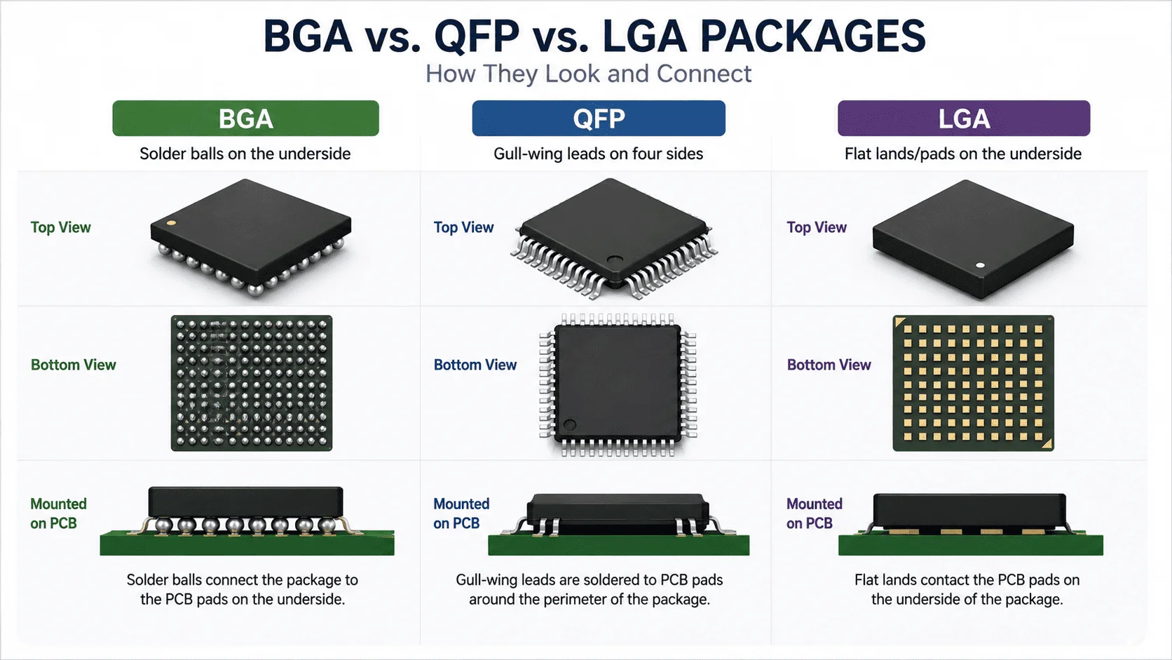
What’s the Difference Between BGA, QFP, and LGA Packages?
| Feature | BGA | QFP | LGA |
| Connection type | Solder balls on the underside | Gull-wing leads on four sides | Flat lands/pads on the underside |
| Contact location | Area array | Perimeter | Area array |
| Pin density | Very high | Moderate | High |
| PCB routing complexity | High | Low | Moderate |
| Footprint efficiency | Very high | Moderate to low | Very high |
| Electrical performance | Excellent | Moderate | Better |
| Thermal performance | Exceptional | Limited | Good, especially in socketed/high-contact designs |
| Inspection method | X-ray / AOI | Visual / microscope | Visual / microscope |
| Reworkability | Harder (hidden joints make repair difficult) | Easier | Easier than BGA |
| Best for | High-speed, high-density ICs | Lower-to-mid pin-count ICs | High-contact-count parts, socketed parts, and some high-performance CPUs |
Bottom Line
The BGA chip is the savior of modern electronics. It has made today’s compact and powerful devices possible in the first place. Spreading connections across the entire underside of the chip has enabled engineers to pack more I/O into smaller spaces, while also unlocking better heat control and cleaner electrical performance.
BGA packaging does require precision assembly and tighter routing. However, none of that is a dealbreaker when you are working with a manufacturing partner like LHD TECH who has the right equipment and process controls in place. Keep these fundamentals in mind, and your next BGA-based design will hold up to the standards modern electronics now demand.