Introduction: PCB Pinner in the World of Electronics
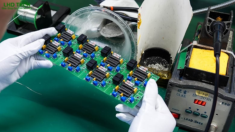
With the rapid development of modern technology, pcb pinner is playing an increasingly important role in the field of electronic manufacturing. Whether you are engaged in pcb assembly or are interested in the complex pcb manufacturing process, you will find that the key lies in:the precise positioning and fixation of components. As is well known, even the slightest deviation during the assembly process can lead to problems such as short circuits and shortened product lifespan. In more serious cases, it can even cause the circuit board to completely fail.
In every successful assembly process—especially for multilayer pcb and through-hole pcb assembly—the pinner plays a crucial role in ensuring that components or circuit board layers are securely fixed, which can fully guarantee the perfect execution of the soldering or bonding processes. Due to the collaboration between PCB manufacturers and designers, which has led to precise positioning solutions, high-reliability and high-performance products such as smartphones, automotive control systems, aerospace avionics equipment, and advanced medical devices can be mass-produced.
What Is a PCB Pinner? The Role of the Pinner in PCB Assembly
A pcb pinner is a type of tool, fixture or equipment specifically used in the pcb assembly process. They are mainly employed for precise positioning, insertion, fixation of pins, components or PCB layers during production, to prevent displacement and shaking, and to ensure the accuracy of soldering and assembly. They are indispensable in both through-hole technology (THT) and surface mount technologies, ensuring that the position of each pin meets the electrical and mechanical performance requirements.
The Core Functions of a PCB Pinner:
- Align and Secure Components: Securely hold the pins, leads and components in place to prevent them from moving around during the mounting and soldering process, ensuring that the positions are within the reasonable tolerance range.
- Enhance Precision: It can achieve precise positioning at the micron level. Even in situations where the boards are densely packed, very small and very complex, it can still easily handle the challenges.
- Prevent Movement or Misalignment: Essential for multilayer pcb—during the processes of lamination, drilling and soldering, it can effectively prevent layer misalignment and parts from falling off.
Who Uses PCB Pinners?
- PCB Manufacturers: The factory can ensure product quality and enhance product competitiveness by using pinners
- Design Engineers: Who require prototype reliability in new pcb design projects
- Electronics Assemblers: The manual positioning tool operator and the automated soldering machine operator can enhance their efficiency by using this tool.
- Quality Control Inspectors: Before the final inspection, use this equipment to confirm that the pins are properly fixed in place.
How Does a PCB Pinner Work? Step-by-Step in Modern Factories

A pcb pinner work process is developed through joint design by manufacturers and assembly engineers. It includes three modes: manual, semi-automatic, and fully automatic. . The specific operation steps are as follows:
Step-by-Step: Typical PCB Pinner Operations
- Board Preparation:
- PCBs with drilled or plated holes (for THT) or prepared pad locations (for SMT) are loaded onto an assembly fixture.
- Component Placement (Pick-and-Place):
- The pins, headers and components are first placed at the fixed positions by manual operation, a surface mount machine or a robotic arm.
- Because the locating pins can align the pins, this enables us to ensure that the leads are precisely aligned with the pads or through holes.
- Alignment and Securing:
- Under the action of mechanical fixtures, vacuum clamps or special tooling, the pins and components will be firmly fixed
- during the pressing and drilling processes of multi-layer PCBs, the positioning pins will fix each layer of the board.
- Soldering or Bonding:
- Precise pin positioning can significantly prevent displacement during soldering, resulting in perfect solder joints. This also reduces the risk of short circuits and enhances production efficiency.
- In reflow soldering or wave soldering production lines, a positioning pin system is usually integrated.
- Inspection and Quality Control:
- High-quality positioning pins will assist in transmitting data to the automatic optical inspection (AOI) system, thereby achieving the purpose of verifying positioning and stability.
- Release and Transfer:
- After soldering is completed, the locating pins release the circuit board, and it proceeds to the final quality inspection and subsequent processes.
Table: PCB Pinner Workflow by Assembly Technology
| Assembly Method | Pin Insertion Tool | Securing Method | Inspection |
| Manual | Manual pinners or tools | Jig/Vacuum clamp | Visual & AOI |
| Semi-Automatic | Pneumatic pinner machine | Jig/Fixture | AOI + Sensors |
| Automatic (SMT/THT lines) | Pick-and-place robots | Robotic fixture | AOI + X-ray |
Using PCB Pinners for Assembly: Ensuring Precision, Alignment, and Quality
Precision during the pcb assembly process is not negotiable, especially for complex or high-density board layouts. Pcb pinners can keep each pin in the correct position, including direct alignment or pin fixation, effectively preventing them from moving due to vibration, heat or operational errors.
Common Ways PCB Pinners Ensure Quality:
- Alignment and Stability: While being compatible with small SMT pads, it also achieves alignment and fixation with long THT pins.
- Component Shapes and Sizes: Modern pcb pinners adapt to various components, from fine-pitch ICs to large power connectors.
- Trusted Across Industries: Widely applied in the fields of aerospace, medicine and automobiles.
Case Study:
A PCB factory specializing in medical instrumentation found that by switching to automatic pinner solutions, post-soldering defects dropped by 41% and time spent on board rework reduced by over 55%.
Key Quality Control Metrics Influenced By Pinners:
- Pin placement accuracy
- Solder joint quality
- Overall defect rate (short circuits, opens, etc.)
Using PCB: Why Using PCB Pinners is Critical in Manufacturing
Real-World Reasons PCB Pinners Are Used:
- Component Safety: Effectively prevent damage to components during reflow soldering and wave soldering processes, thereby extending the service life of the components.
- Speed and Efficiency: Under the condition that the components are securely fixed, the throughput efficiency of automated assembly and soldering can be significantly improved.
- Reduced Defects: Reduce the probability of manual rework and product returns, lower the after-sales costs, and enhance production efficiency.
- Ideal for Multilayer and Hybrid PCBs: Perfectly integrated with high-density interconnection (HDI), multi-layer boards and hybrid process layouts.
Pinners in PCB Assembly: The Crucial Role in Component Placement
Pinners Play a Crucial Role in:
- Every Board and Layer: Whether it is a single-panel, double-panel or multi-layer board, it can be perfectly adapted. Ensure that all the components are positioned accurately.
- Maintaining Electrical and Mechanical Performance: It can support tens of thousands of cycles of use and meet the requirements of fields such as aerospace and defense.
- Collaboration between PCB Teams: It can help the design, assembly and quality inspection teams work closely together to enhance work efficiency and achieve the best positioning effect.
Where Pinners Are Used in the PCB Assembly Process
| Process Stage | How PCB Pinners Help |
| Prototyping | It can flexibly adapt to different pin quantities and shapes, and quickly respond to changes in circuit board layout and special component requirements. |
| Automated SMT Assembly | Help with alignment and fixation of small and fragile components before and after reflow soldering, preventing displacement and deviation, and achieving precise positioning. |
| Through-Hole Assembly | Pinner ensures leads that pass through the board are precisely aligned for reliable soldering, essential for through-hole pcb assembly with heavy or high-power components. |
| Multilayer Stack-Up | During the pressing, drilling and copper plating processes, the layers can be accurately aligned to ensure that the over-hole positioning is not affected by layer misalignment. |
| Final Inspection | Pinners can fix the circuit board for AOI (Automatic Optical Inspection) or ICT (In-Circuit Test), thereby avoiding inspection errors caused by component displacement and board bending. |
PCB pinners play a crucial role in every stage of the manufacturing process, from the initial prototype to mass production in pcb factories. By ensuring alignment and stability during assembly, pinners reduce defects and lead to higher product reliability.
Pinner in PCB Manufacturing: Solutions Across Technologies
The pinner in pcb manufacturing must adapt to evolving board technologies, changing component shapes, and tighter tolerances in modern electronics.
Through-Hole vs. SMT: Two Paths, One Goal
| Technology | Main Challenge | How PCB Pinners Help |
| Through-Hole Technology | Ensuring long leads stay aligned during insertion and soldering | By fixing the pins, it prevents tilting, ensures the formation of the solder joints, and thus avoids short circuits. |
| Surface Mount Technology | Placing components directly onto the pcb surface at micron-level accuracy | Pinners can help fix the tiny components before and after reflow soldering, preventing defects such as protrusion or deviation. |
| Hybrid / Multilayer Boards | Combining SMT and THT on one board, managing complex stack-ups | The locating pins can ensure precise alignment of all pins, components and layers. |
Modern pcb pinners are often integrated into automated pick-and-place machines and soldering stations, providing adaptive fixturing for improved process control and fewer operator interventions.
Advances in Pinner Solutions
- By attaching high-precision positioning pins to sensors or vision systems, the alignment status of the pins before assembly can be verified.
- Some positioning systems are jointly developed by PCB manufacturers and equipment providers, and they can be applied in various fields, such as aerospace and healthcare industries.
- For plates with flexible or irregular shapes, more and more customized fixture heads or devices based on the principle of vacuum are being adopted.
Benefits of PCB Pinners: Building Reliable and Efficient Boards
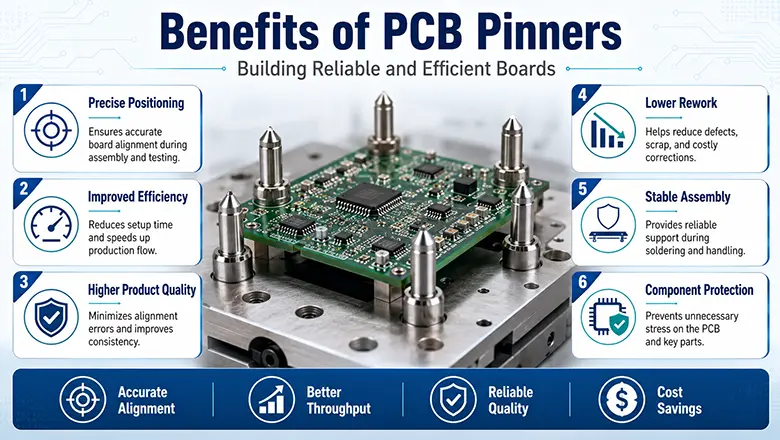
Optimizing the use of pcb pinners leads to significant benefits across every assembly process:
Key Benefits of PCB Pinners
- Maximum Precision: Ensure that all pins, components and board layers are accurately aligned and fixed, thereby reducing rework and improving the quality of the finished product.
- Faster Manufacturing Process: The surface mount machine and the soldering equipment can operate at full capacity, reducing the downtime for debugging and maintenance, and improving efficiency.
- Defect Reduction: Avoid problems such as bridge soldering, circuit breakage, and pin misalignment, and reduce the possibility of short circuits and on-site failures.
- Supports Complex Board Layouts: For high-density, multi-layer printed circuit boards, this is of utmost importance because even the slightest deviation could cause the entire circuit board to malfunction.
- Reliability and Consistency: By minimizing long-term failures caused by vibrations to the greatest extent, ensure that the product has long-term reliability, especially in harsh environments (such as in automobiles, aviation, and defense sectors).
Types of PCB Pinners and Pin Solutions
Different assembly processes correspond to different types of locating pins:
Manual Pinners
- Used for prototype production or small-scale manufacturing.
- Adaptation to special-shaped components and rapid design changes.
- Achieving the best results requires industry experience.
Semi-Automatic and Automatic PCB Pinners
- Used in pcb factories for mass production.
- Quickly switch the circuit board models to meet the requirements of high production capacity and high consistency.
- Often used in combination with robotic arms and visual guidance assembly systems.
Customized and Hybrid Pinner Solutions
- Adapted for special layouts, flexible PCBs, and mixed circuits boards combining SMT and THT technologies.
- It was jointly developed by PCB manufacturing engineers and equipment manufacturers.
Choosing the Right PCB Pinner
| PCB Application | Recommended Pinner Type | When to Use |
| Prototyping/Lab | Manual / Customized fixtures | For short runs, varied components |
| High-Volume SMTA | Automatic/Robotic | Large batches with standard components |
| Aerospace/Medical | High-Precision, with AOI | Where reliability and traceability are critical |
| Flexible/Curved PCB | Custom Vacuum/Soft Fixture | Odd shapes or flex circuits |
Best Practices for High-Quality PCB Assembly Using PCB Pinners
- Early Design Review: Ensure all teams, from pcb design to assembly and AOI inspection, are aligned on pin positioning and access, especially for complex or multilayer pcb.
- Appropriate Fixturing: The positioning pins can be selected as manual, automatic or hybrid based on the production volume and the complexity of the circuit board.
- Routine Calibration and Maintenance: Maintaining a well-functioning positioning system can reduce deviations during long production runs.
- Continuous Training: Whether using manual pinners or supervising robot-driven lines, well-trained staff catch misalignment or tool wear early in the process.
- Regular AOI Feedback: Integrate feedback loops from optical inspection and in-circuit testing back to pinning setup for continued process improvement.
Common Challenges — And How PCB Pinners Help Reduce Defects
Challenges in PCB Assembly
- Movement Before Soldering: If there is no suitable locating pin, even a slight vibration can cause the lead to shift, resulting in bridging or short circuit.
- Irregular Component Shapes: Special packaging requires the use of a corresponding fixing head to align and secure the components during the assembly process.
- Increasing Miniaturization: A tighter spacing means that even the slightest deviation could cause damage to the circuit board, especially in the design of high-speed multi-layer printed circuit boards.
- Multiple Board Layers: Keeping each layer registered during lamination and drilling relies on high-accuracy pinner solutions.
Solutions and Defect Reduction
Using pcb pinners helps:
- Minimize handling defects (bent pins, missing components).
- Reduce solder shorts or weak joints.
- Achieve precise fixation of the circuit board, accelerating AOI and testing quality inspection.
- Boost yield and product quality, ultimately reducing total cost of ownership for every batch produced.
FAQs: PCB Pinners, Pin Placement, and Reliable Boards
Q: What is the main reason to use a pcb pinner in pcb manufacturing?
A: Ensure that all pins, leads, and board layers are precisely positioned to guarantee the firmness of the soldering and the reliability of the mechanical connection.
Q: Are PCB pinners only used for through-hole pcb assembly?
A: No. Originally designed for through-hole technology, but modern locating pins now cover SMT, HDI, multi-layer boards, and mixed-process circuit boards, and can fix the smallest surface-mounted components.
Q: How do pcb pinners ensure product reliability?
A: By preventing movement during critical assembly steps—soldering, cooling, or inspection—pcb pinners ensure the board quality matches the intent of the pcb design and reduces defects that would otherwise escape detection.
Q: Can I use manual pinners for high-volume production?
A: In mass production, in order to achieve the best yield and consistency of printed circuit boards, it is strongly recommended to use automated or semi-automatic pick-and-place machines. However, for prototype production, custom assembly, or situations where design changes need to be made frequently, manual solutions are more appropriate.
Q: What’s the link between pinners and collaboration between pcb teams?
A: The best pinner solutions are developed through collaboration between pcb design, assembly engineering, and manufacturing. This team approach leads to easier assembly, improved manufacturability, and fewer defects.
Conclusion: The Ongoing Evolution of PCB Pinner Solutions
In summary, the pcb pinner is a foundational tool in the evolution of high-quality, reliable, and efficient electronic products. As circuit complexity rises, board layouts become denser, and demand for flawless performance increases, pinners in pcb assembly have become even more essential.
Pinners play a crucial role not just in aligning and securing components or layers, but in reducing defects, improving precision, and ensuring the quality of the final board—regardless of industry. The advanced, automated, and customized locating solutions jointly developed by manufacturers and designers continuously promote the upgrade of PCB production capacity.
For PCB manufacturers and designers, investing in modern locating pins, following usage guidelines, and conducting staff training can lead to significant returns in terms of yield, defect control, and customer satisfaction. Every reliable PCB begins with precision, and this precision starts with the selection and proper use of locating pins.
With the advancement of manufacturing technology, the role of locating pins has been continuously evolving. From manual locating pins used in laboratory prototypes to robotic positioning systems in fully automated PCB factories, the core of the future remains the precise alignment and fixation of components throughout the entire manufacturing process.
The locating pins used in PCB assembly are not merely tools; they are also the reducers of defects, the guarantors of quality, and the contributors of data for intelligent factories. As more surface mounters, soldering equipment, and AOI systems are interconnected, the locating pins will become the key bridge connecting the reliability of manual design and machine manufacturing.