
Introduction
The demand for reliable, high-performance electronics has never been higher. In today’s fast-paced manufacturing environment—where miniaturization, complex PCB design, and surface mount technology (SMT) standards dominate—solder paste inspection (SPI) is the essential inspection technique that ensures every pcb assembly meets the highest standards. SPI, especially when leveraging advanced 3d spi, is central to the success of every product, from smartphones to automotive controls.
Imagine a world where one tiny defect in a solder paste deposit could bring down an entire device. That’s why leading manufacturers rely on 3D solder paste inspection and intelligent spi machines: to detect, analyze, and prevent even the smallest issues in the solder paste printing process.
In this comprehensive guide, we’ll explore how SPI works, why it’s essential, what defects it catches, and how integrating SPI with modern inspection processes and Industry 4.0 can future-proof your operation. We’ll show you why SPI is the backbone of pcb assembly quality, and how 3D SPI provides unbeatable assurance compared to traditional visual checks.
What is Solder Paste Inspection (SPI)?

Solder Paste Inspection (SPI) is an automated, precision inspection method focused on evaluating the quality of every solder paste deposit produced during the printing process on a PCB. By utilizing sophisticated optics and, in the latest systems, 3D (three-dimensional) imaging, SPI measures solder paste volume, solder paste height, area, and alignment. Modern SPI systems provide fast feedback and closed-loop process control, allowing adjustment of the solder paste printer or stencil in real time to maintain optimal process quality.
Key Purposes SPI Serves:
- Detect solder paste defects (insufficient solder, excess solder, bridging, misalignment)
- Measure solder paste volume accurately on every pad
- Prevent solder joint failures by catching paste errors early
- Improve overall pcb quality and reliability
- Enable yield improvement and process control using real-time spi data
A state-of-the-art spi machine can inspect hundreds of boards per hour, automatically categorizing results, and delivering actionable insights for operators and process engineers.
Why is Solder Paste Inspection (SPI) Essential in Modern PCB Assembly?

Solder paste printing is the “point of no return” for SMT quality. More than 60% of SMT defects originate from improper solder paste application, making SPI the most essential inspection for manufacturers who care about pcb quality.
Why SPI Inspection is Non-Negotiable:
- Catches Issues Before Component Placement SPI helps manufacturers inspect the solder paste immediately after the paste deposition step. Defects like insufficient paste, misalignment, or incorrect height can be reworked before any components are mounted.
- Prevents Weak Solder and Field Failures SPI ensures only printed boards meeting precise standards move forward, which greatly reduces the rate of weak solder joints or random field failures.
- Supports Advanced PCB Design Modern pcb assembly uses fine-pitch components, micro-BGAs, and 01005s that demand exact volume of solder paste. Only advanced 3d spi systems can consistently handle the measurement requirements at this scale.
- Feeds Process Control and Improvement By integrating SPI data with MES, engineers can spot when a solder paste printer or stencil begins to drift out of spec or needs cleaning.
How Does Solder Paste Inspection (SPI) Work? Process and Key Steps

Step-by-Step SPI Operation in SMT Lines
Solder Paste Printing
- Solder paste is applied to PCB pads via a precision stencil and a paste printer. The quality of solder paste printing is crucial for subsequent steps.
Automatic Board Transfer to SPI Machine
- Boards are transported via conveyor to the spi machine while the paste is fresh.
3D Imaging and Measurement
- Advanced 3d spi systems use fringe light, lasers, or structured light to create a 3D map of every paste deposit. This allows the system to measure solder paste volume, solder paste height, area, and alignment with high accuracy.
Comparison to Reference Data
- SPI software compares the live inspection results to reference CAD/Gerber data. Misalignments, volume deviations, and shape anomalies are flagged instantly.
Real-Time Classification and Feedback
- The SPI machine classifies deposits as “Pass” or “Fail” and, in closed-loop setups, automatically feeds back data to the solder paste printer for process corrections.
Core Elements in a 3D SPI Machine
| Component | Function |
| High-Resolution Cameras | Capture 2D and 3D images of each paste deposit |
| Laser/Structured Light Optics | Enables accurate solder and paste measurement in 3D |
| Transport & Conveyor | Automates board handling for high throughput |
| SPI Software | Analyzes, logs, and visualizes inspection results |
| MES/Analytics Integration | Shares SPI data for traceability, SPC, and process control |
Key Parameters in SPI: Solder Paste Volume, Height, Alignment, and Area
SPI measures solder paste deposits across several critical parameters—ensuring each contributes to a trustworthy solder joint.
1. Solder Paste Volume
The amount of solder in each deposit is measured in cubic microns. Insufficient solder or excess solder are common culprits for reliability failures. SPI focuses on maintaining volume tolerance—typically ±15% of the target value.
2. Solder Paste Height
A less obvious, but equally vital measurement. Variations in height can cause component seating problems or promote tombstoning during reflow. Only modern 3d spi technology can reliably gauge this parameter.
3. Solder Paste Area
Ensuring that solder paste deposits cover the required pad area without overflowing is crucial for good solder adhesion and proper wetting. If the paste covers too little area, insufficient solder or weak joints can result. If it covers too much, it can lead to excessive paste, risking shorts when the volume of solder melts and spreads during reflow. SPI systems provide high-precision mapping of every deposit’s area, ensuring every pad is correctly covered.
4. Solder Paste Alignment
Proper alignment is vital in modern pcb assembly where components are often densely packed. Even a perfectly measured amount of solder paste is risky if the deposits aren’t properly centered. Misaligned deposits may not form reliable solder joints or could cause bridging and shorts. With 3d solder paste inspection, even minimal misalignments are quickly flagged—allowing process adjustments before errors become costly.
The Importance of Consistent Paste Deposits
A successful printing process delivers thousands of precisely measured, correctly aligned solder paste deposits every hour. SPI prevents defects by ensuring this consistency—you can evaluate solder paste deposits in real time, maintain solder quality, and catch ever-subtler shifts before they cause escapes.
Defect Detection: Common Issues SPI Prevents
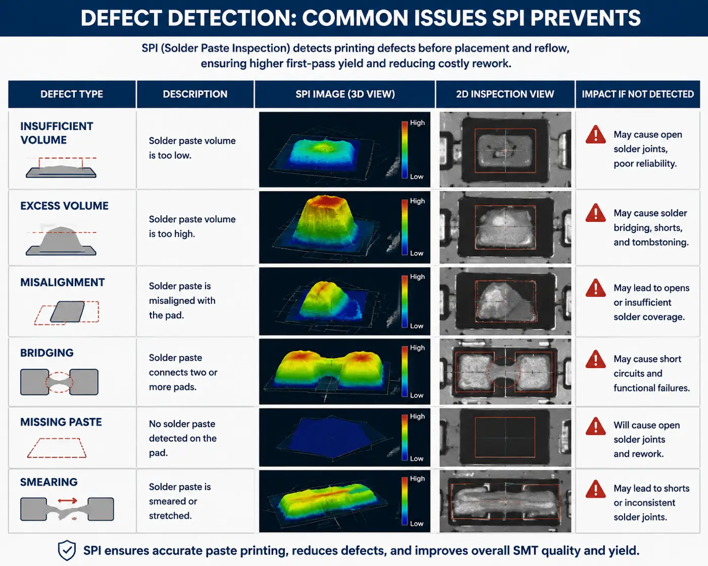
SPI helps manufacturers catch and prevent the most frequent and damaging solder defects, including:
1. Insufficient Solder Paste / Insufficient Solder
SPI detects deposits that are too small, thin, or otherwise below process thresholds, flagging them as insufficient paste or insufficient solder. These are the classic root causes for cold joints, intermittent connections, and rework headaches.
2. Excess Solder / Excess Solder Paste
Too large a volume of paste can result in excessive solder and shorts, especially when reflow allows solder to bridge between pads.
3. Bridging
When excess or misaligned solder paste bridges adjacent pads, it causes shorts and catastrophic failures. SPI catches these in real time—before components are placed, reducing the risk and saving money.
4. Misalignment and Shape Deformation
Off-center deposits or uneven paste shapes are common when stencils wear or printers drift out of calibration. Any such anomaly can cause tombstoning, misplaced components, or weak solder joints.
5. Voids and Poor Wetting
Some advanced 3d spi machines can also catch issues like air bubbles (voids) in the paste or surface defects that may compromise solderability during reflow.
Table: Examples of Solder Paste Defects and Impact on PCB Quality
| Defect Type | Detected By | Typical Impact |
| Insufficient solder paste | SPI measures paste volume/area | Opens, weak or unreliable joints |
| Excessive paste/solder | SPI height/volume analysis | Shorts, bridging, excess solder balls |
| Misaligned paste | XY offset in SPI inspection | Tombstoning, failed pads |
| Paste shape deformities | 3D SPI mapping | Irregular joints, poor wetting |
| Voids or skips | 3D SPI & optical inspection | Random failures, poor solder quality |
Advanced 3d spi technology allows process engineers to not only find but also classify the subtle distinctions between these issues, improving the evaluation of solder performance for every assembly.
SPI Technology: 2D SPI vs 3D SPI vs Advanced 3D SPI Machines
2D SPI Systems
Traditional 2d spi systems use flat, top-down views to measure paste area and some offset. While they’re still in use for legacy applications and boards with large features, they cannot measure solder paste volume or solder paste height reliably. As a result, they often miss subtle but critical defects—especially in modern pcb design environments favoring micro-BGAs and fine-pitch parts.
3D SPI Systems
3d spi and advanced 3d spi machines represent the industry gold standard. They utilize fringe projection, structured light, or lasers to inspect the solder paste in three dimensions—giving accurate readings of paste deposit height, area, and volume. With these measurements, process engineers have the actionable data they need to ensure precise solder paste application and reliable assembly every time.
Advanced 3D SPI
Advanced 3d spi technology offers features like automatic warpage compensation (for flexible circuits), AI-powered defect classification, and easy integration with MES, SPC, and printer feedback systems. These platforms are not only fast and accurate but are also the backbone of Industry 4.0 initiatives for high-end manufacturers.
Table: 2D SPI vs 3D SPI vs Advanced 3D SPI
| Feature/Capability | 2D SPI | 3D SPI | Advanced 3D SPI |
| Measures solder paste area | Yes | Yes | Yes |
| Measures solder paste volume | No | Yes | Yes (micron-level repeatability) |
| Detects misalignment | Yes | Yes | Yes |
| Detects solder height/shape | No | Yes | Yes (with advanced shape analysis) |
| Industry 4.0 integration | No | Limited | Yes (cloud/analytics ready) |
| Suitable for HDI, fine-pitch | No | Yes | Ideal |
| Prevent solder defects | Limited | Yes | Superior |
Modern 3d spi delivers accurate, actionable feedback—in real time—enabling both operators and closed-loop systems to maintain ideal process conditions.
Essential Tips for SPI Operation & Optimizing Inspection Processes
- Set Realistic Tolerances: Your spi software should match tolerances to product requirements. Overly tight thresholds create false positives; loose tolerances can miss real defects.
- Review and Interpret SPI Data Daily: Integrating SPI results with your MES or production dashboard helps spot subtle process drift or trends before they create escapes.
- Calibrate Regularly: Both the SPI machine and solder paste printer require regular calibration for accurate results—especially when changing solder paste, board designs, or stencil types.
- Utilize Color-coded Inspection Results: Modern SPI platforms provide easy-to-read 3D and heatmap visualizations—use these daily to quickly verify process health.
- Automate Feedback Loops: Where possible, connect your SPI to the solder paste printer to adjust blade pressure, speed, or stencil cleaning automatically based on inspection data.
SPI in Action: Real-World Scenarios & Case Studies
Automotive: Preventing Recall Disaster
An EMS serving the automotive sector replaced failing AOI with 3d solder paste inspection on airbag controller boards. By focusing on early accurate solder volume and detecting subtle stencil wear, SPI helped stop over 80% of previously undetected bridging issues—contributing directly to safety and compliance.
Wearables: Cutting Field Returns
A global wearable device leader saw high field returns from weak solder joints on micro-LED arrays. Enhanced SPI measurements of solder paste height and area, alongside AI-driven process tuning, halved random failures and boosted customer trust.
Key Factors Affecting Solder Paste Printing Quality and SPI Accuracy
Solder paste printing quality is influenced by:
- Stencil aperture geometry and wear (affects paste release and deposit formation)
- Solder paste rheology (viscosity and particle size)
- Environmental controls (temperature and humidity can change solder volume outcomes)
- Operator training (skilled staff interpret results, spot trends, and keep lines running at peak quality)
- Printer and SPI calibration (out-of-tune machines create measurement bias or drift)
Leveraging SPI Data for Process Optimization & Industry 4.0 Integration
SPI systems provide more than binary pass/fail decisions. Every spi inspection generates a wealth of inspection data—height, solder paste volume, area, offset, and even 3D shape.
How to Use This Data:
- Monitor trends: Identify slow stencil degradation before major defects occur.
- Enable closed-loop feedback: Automate printer adjustments for volume, pressure, and cleaning.
- SPC and process improvement: Use standard deviations, Cp, Cpk indices for ongoing production quality measurement.
- Global consistency: In distributed manufacturing, cloud-based SPI data ensure standards are followed worldwide, not just at one facility.
SPI enables advanced SPC dashboards, predictive analytics, and proactive maintenance—powerful levers for any PCB manufacturing operation targeting world-class yield.
Best Practices for SPI and Solder Paste Measurement
- Calibrate regularly Every time you change board size, paste type, or stencil, recalibration maintains measurement accuracy.
- Correlate SPI and AOI data for root cause analysis.
- Adopt recipe management for quick changeovers between PCB designs.
- Train operators to distinguish between genuine defects and process noise.
- Update inspection methods as new components and board layouts are introduced, particularly when moving to HDI boards or ultra-fine pitch devices—a scenario where 3d spi or even more advanced 3d spi technology truly excels.
- Archive inspection data for trend analysis. Persistently storing SPI results helps in identifying gradual changes, such as decreasing solder paste release efficiency, which might indicate stencil clogging or degradation in solder paste quality.
- Use statistical process control (SPC) tools to monitor Cp and Cpk indices for all critical parameters like solder paste volume, solder paste height, and alignment. Maintain these indices above industry benchmarks (typically 1.33 or higher), which is key for robust and repeatable pcb assembly.
- Integrate SPI with other essential inspection processes like AOI and X-ray. By cross-referencing SPI inspection results with downstream inspection processes, you gain deeper insights into how early solder paste defects impact final assembly and solder joint reliability.
Challenges in SPI and Modern Solutions
Despite the power of spi solder paste inspection, several challenges can limit its effectiveness if not addressed:
- Miniaturization & Complex PCB Design: Ultra-fine pitch and small pad sizes found in micro-BGA or 01005 assemblies require the high resolution and advanced image processing of advanced 3d spi machines. Traditional 2d spi systems may miss subtle height or volume differences in these scenarios.
- Flexible & Warped PCBs: Boards may distort during handling, skewing measurements. Modern 3d spi provides warpage compensation to maintain accurate solder paste measurement.
- Opaque/Reflective Surfaces: Some pcb finishes reflect or scatter inspection light, affecting accuracy. Choose spi machines with adaptive lighting or advanced 3d algorithms to handle these cases.
- Human Factors & Training: Operators must interpret spi data correctly and respond effectively to inspection results. Regular training and clear SOPs help reduce the risk of false positives and raises overall solder quality.
- Process Integration: Integrating spi with AOI, MES, and process feedback loops can be challenging in legacy factories. However, manufacturers are increasingly investing in seamless data flow between the solder paste printer, spi machine, and analytics platforms for complete assembly line control.
SPI vs Automated Optical Inspection (AOI): Essential Inspection Synergy
It’s important to understand that SPI and AOI are complementary, not interchangeable. This SPI vs AOI comparison clarifies their unique strengths:
| Characteristic | SPI (Solder Paste Inspection) | AOI (Automated Optical Inspection) |
| Focus | Printed solder paste/pre-reflow | Components & solder joints/post-reflow |
| Detects | Paste volume, area, height, alignment | Missing/skewed parts, soldering defects |
| Prevents | Solder paste defects before assembly | Assembly & final solder joint defects |
| Timing | After solder paste printing | After reflow soldering |
| Technology | 3d spi, advanced 3d, optical inspection | 2d/3d optical inspection, X-ray |
The essential inspection sequence is: SPI ensures your solder paste process is stable and deposits are perfect. AOI verifies all components are correctly placed and reliable solder joints are formed after reflow. For the highest pcb quality, both systems should be operating in tandem, providing “bookends” to the SMT process.
The Future of Solder Paste Inspection: AI, Cloud, and Predictive Analytics
- Advanced spi and modern 3d spi systems are rapidly adopting technologies that will transform assembly lines:
- AI & Machine Learning: Adaptive SPI detects unusual or rare defects, such as pattern-based issues, using deep learning. It can also auto-tune spi software tolerances to balance false positives and escapes.
- Cloud-Based SPI Data: Manufacturers can compare process performance globally. Instant data sharing between facilities ensures that best practices are adopted worldwide, improving consistency and boosting pcb assembly competitiveness.
- Predictive Analytics: SPI data not only highlights present defects but also anticipates halts or failures before they occur (e.g. predicting when a stencil will need cleaning or replacement).
- IoT and MES Integration: SPI is a critical node in Industry 4.0 smart factories. Inspection results, trends, and anomalies communicate directly with MES to fine-tune line performance in real time.
Frequently Asked Questions: SPI, 3D SPI, and PCB Quality
Q: How does SPI prevent solder defects from affecting final pcb quality?
A: By catching deviations in solder volume, paste deposit height, and alignment before component placement, SPI prevents process escapes, ensuring only boards with precise solder paste printing proceed.
Q: Are 2d spi systems still adequate for today’s pcb assembly?
A: For simple, low-density assemblies, yes. For HDI, miniaturized, or mission-critical products, advanced 3d spi machines are the clear choice due to their ability to capture subtle variations in height and solder paste deposition.
Q: How does integrating SPI help with continuous improvement?
A: Integrating SPI with MES or data analytics platforms delivers full traceability and enables robust SPC. Engineers can monitor process trends, optimize the printing process, and respond to issues before they escalate.
Q: Can SPI measurement influence stencil design?
A: Absolutely—reviewing visual and statistical SPI data allows process engineers to optimize aperture sizes, shapes, and board orientation, directly influencing future stencil and pcb design.
Get the SPI Edge: Partner with Us for Superior PCB Assembly and Reliable Solder Joints
As a trusted expert in SMT and spi inspection, we’ve helped hundreds of manufacturers implement the most advanced 3d and 3d spi technology available. Here’s what sets our team apart:
- Tailored SPI solutions: From selecting the right spi machine and configuring spi software recipes to training your operators for exceptional inspection results.
- Yield-first approach: Our process is focused on eliminating solder defects, maximizing the quality of solder paste printing, and delivering reliable solder joints every time.
- Full Industry 4.0 integration: We help you link SPI, AOI, X-ray, and MES to get real-time actionable insights and predictive analytics.
- Comprehensive support: From evaluation of solder to post-install process audits and remote troubleshooting.
Conclusion: SPI Ensures Reliable Solder Joints and PCB Quality
SPI prevents defects at the source—right after solder paste printing and before a single component is placed. It is an essential inspection stage for any modern SMT operation. Thanks to advanced 3d spi and the integration of spi with real-time analytics, manufacturers now achieve:
- Measurable improvements in first-pass yield
- Highly reliable solder joints and robust product deliveries
- Lower warranty costs and increased market trust
If you’re striving for zero defects, spi solder paste inspection supported by advanced 3d spi machines—and smart, actionable spi data—is non-negotiable. Integrate SPI as the cornerstone of your essential inspection strategy and watch your process capability, customer satisfaction, and competitiveness grow.