Introduction
The electronics manufacturing industry is rapidly evolving. Practitioners must deeply understand the core distinction between PCB and PCBA. These practitioners are involved in circuit design, product development or actual production. During the process of building electronic devices, many easily overlook a critical step. They fail to differentiate between a bare board and a fully assembled circuit board component. A PCB refers to a printed circuit board without components installed. A PCBA is a circuit board assembly with all components soldered and mounted. The distinction between them directly influences design decisions and manufacturing strategies. This impact extends further to the final quality level of the product. It also relates to the overall control of production costs and the time cycle required for product launch.
Whether you are a design engineer, procurement manager or electronics entrepreneur, this article will help you learn the critical differences and roles in electronics manufacturing for both PCBs and PCBAs. We’ll walk you through every major stage in the circuit board manufacturing process, from prototyping to mass production, including PCB fabrication, assembly, quality control and the nuances that influence the cost of PCBA versus a simple flat board made for early prototyping.
By the end, you’ll understand the difference as well as how to work with a good PCB manufacturer, select between bare PCB or turnkey PCBA service and optimize your production volume, cost and product quality.
PCB vs. PCBA Overview

Let’s start by understanding the distinction between PCB vs. PCBA—a foundation for all stages in electronics manufacturing.
- PCB (Printed Circuit Board):This is a flat board made of an insulating substrate, usually FR4 glass epoxy or similar PCB material, with copper traces etched to form the required circuit pattern. A PCB is a bare circuit board with no electronic components mounted. Think of it as the skeleton—a map of your electronic circuit, waiting to be populated.
- PCBA (Printed Circuit Board Assembly):Once electronic components are soldered onto the board, the PCB becomes a PCBA. Now, both passive and active components—resistors, capacitors, ICs—are assembled onto the PCB, forming a complete circuit board. The PCBA is the finished product that powers your smartphone, car or medical monitor.
Roles in Electronics Manufacturing
It is a core professional essential requirement for all operational links in the entire electronic manufacturing production process that practitioners in the electronic manufacturing industry grasp the core essential differences between PCB and PCBA:
- PCB fabrication defines the circuit’s structural and electrical foundation, while
- PCB assembly (PCBA process) brings the circuit to life by adding the necessary electronic components onto the PCB, turning a design into a fully functional device.
Why Does the Distinction Matter?
- Assembly Labor and Cost:The assembly of a PCBA involves configuring pick-and-place machines, soldering, manual labor and advanced testing—each step adding value and cost.
- Manufacturing Process:The manufacturing and assembly of a PCB is a technical process that is distinctly separate from the assembly services required to produce a functional PCBA.
- Production Volume:Different suppliers, skills and timelines are needed for producing thousands of bare PCBs versus fully assembled multi-layer PCBA modules.
- Design for Manufacturing:Design considerations for a bare PCB differ from those for a fully assembled PCBA, including component placement, heat dissipation and testability points.
What is a PCB? (Printed Circuit Board)
Definition and Purpose
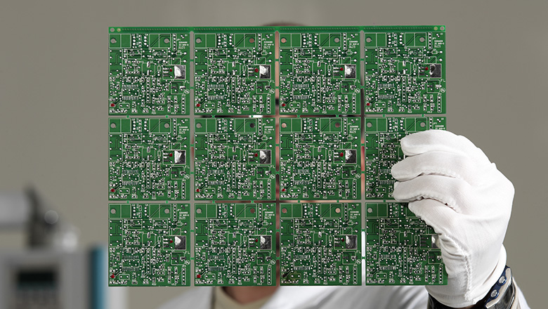
Printed Circuit Boards serve as the fundamental core components of all modern electronic devices and are commonly referred to as bare boards. Structurally, they are flat panels made from specific substrate materials such as FR4, with their surfaces coated by copper layers. These copper layers are precision-etched to form predesigned circuit trace patterns.
Critical Differences:
- The PCB is devoid of any active or passive components.
- It provides the mechanical foundation for components to be assembled and defines the topology of the electrical connections.
Roles in Electronics Manufacturing
- Guides the arrangement and flow of signals through the electronic device.
- Provides mounting surfaces (known as PCB pads) for all components on the board.
- Establishes robust ground and power planes in complex designs.
Manufacturing Process
Let’s break down the PCB fabrication and assembly lifecycle:
1. Circuit Design and Gerber Files
- The initial step is circuit design in specialized EDA software, culminating in the generation of Gerber files—the digital blueprint that defines copper layers, drill data, solder mask and silkscreen.
- Designing the PCB is a critical phase—every routing choice influences manufacturing yield and future assembly.
2. Fabrication Process
- The fabrication process starts by laminating copper sheets onto the PCB substrate.
- Using photolithography, the desired circuit pattern is exposed, developed and etched, forming the traces and pads visible on the surface of the board.
3. Drilling and Plating
- Automated drills make holes (vias) through the board—allowing connections between layers and for component leads in through-hole designs.
- Plating lines coat holes with copper to electrically connect layers in multi-layer PCB
4. Solder Mask and Silkscreen
- A protective solder mask is applied to insulate the copper, exposing only the PCB pads for soldering.
- The silkscreen adds orientation and reference markings directly onto the PCB.
5. Finishing and Testing
- To enhance solderability, finishes like HASL or ENIG are applied to exposed copper.
- The bare PCB is inspected using electrical and automated optical tests to guarantee there are no shorts or open circuits—a hallmark of a good PCB.
Types, Materials and Applications
Types of PCB Boards
- Single-layer PCB: This solution is suitable for the practical application scenarios of high-volume production with low-cost characteristics, and its typical applicable product scope includes power supply products and calculators.
- Simple Two-layer PCB: Offers better routing for more complex circuits.
- Multi-layer PCB: The laminated structure is constructed by the mutual alternating arrangement of substrate layers and copper layers, it has a variety of layer configuration forms including 4 layers, 6 layers and more than 24 layers, and it serves as the core application configuration adopted in the production and manufacturing processes of server motherboards, smartphones and telecommunications equipment.
- Rigid and Flexible PCB:Advanced designs use rigid-flex PCB construction, combining sturdy and flexible segments for wearable and medical uses.
- Aluminum, Ceramic and High Frequency/HDI PCBs:Specialized for power electronics, high-frequency RF and harsh environments.
Common PCB Materials
| PCB Material | Best Use | Features & Benefits |
| FR4 | General Electronics | Good electrical, thermal and cost balance |
| Polyimide | Flexible, high-temperature | Great for flex circuits/harsh settings |
| Aluminum | Power, LEDs | Efficient thermal management |
| CEM-1/CEM-3 | Low-cost PCB designs | Budget-friendly alternatives |
Designing the PCB: Tips and Mistakes to Avoid
- Always design with assembly in mind: enough clearance for components, logical placement for heat and EMI and accessible test points.
- Confirm with PCB manufacturer capabilities: drill sizes, trace width and preferred stackup for high reliability.
- Keep documentation up-to-date, especially when making revisions for production volume or assembly changes—misaligned files are a leading cause of delay in electronics manufacturing.
- Personnel involved in each stage of the electronic manufacturing process bear an irreplaceable core necessity for the understanding of the core differences between printed circuit boards (PCBs) and printed circuit board assemblies (PCBAs).
- Incorporate Design for Manufacturing (DFM) and Design for Assembly (DFA) checks to catch issues before fabrication starts. This ensures your bare PCB transitions smoothly into a fully assembled PCBA, minimizing costly errors.
- Consider thermal reliefs on ground/power planes to ease soldering and prevent component tombstoning.
What is a PCBA? (Printed Circuit Board Assembly)
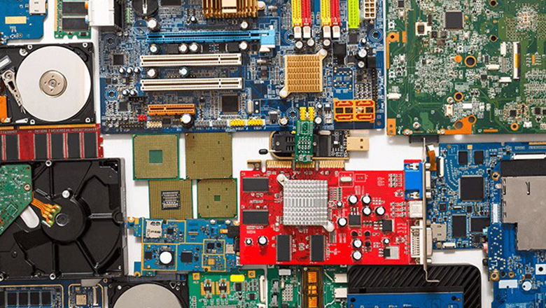
A Printed Circuit Board Assembly (PCBA) is the core development stage with the attribute of subsequent transformation in the field of electronic device research and development. The operators conduct the professional mounting operation of all necessary electronic components for bare printed circuit boards, and by virtue of the rigorously designed production processes and assembly processes, the operators manufacture fully functional circuit boards that can be directly integrated into the interior of various electronic products.
The fundamental distinction between PCB and PCBA lies in their product form and manufacturing stage: a PCB is a printed circuit board without any electronic components installed, serving as a basic semi-finished product in the electronics manufacturing process; whereas a PCBA is a fully functional circuit board that has completed all component placement and soldering processes and passed final quality inspection.
Step-by-Step PCBA Assembly Process
Component Sourcing and BOM Preparation
Begin with a complete Bill of Materials (BOM). Proactively verify the availability, authenticity, and lead time for every item on the list.
Experienced industry suppliers provide professional operation-oriented supply chain management supporting services for the scenarios of turnkey full-process PCBA services and high-volume electronic assembly businesses, and thus effectively mitigate various production and operational risks such as component shortages and counterfeit components.
Stencil & Solder Paste Application
A steel stencil is used to apply solder paste onto the PCB pads—the landing areas for SMT components on the surface of the board.
Component Placement (SMT and THT)
High-speed pick-and-place machines accurately position surface-mount devices onto the PCB. Heavier or mechanical parts may be mounted manually.
Soldering Process
Reflow soldering: The entire assembly is evenly heated in a reflow oven so the solder paste melts and secures components onto the PCB.
Wave soldering: Primarily for THT (through-hole) parts, the board passes over a standing wave of molten solder, bonding leads to the board in one swift movement.
Some boards use mixed technology, with both SMT and THT on different sides of the board for design efficiency.
Inspection and Testing
Automated Optical Inspection (AOI): Verifies all components are in the correct location, with proper orientation and solder joints.
In-circuit testing (ICT): Electrical contact probes confirm circuit continuity and correct values.
Functional testing: The assembled PCBA undergoes power and system-level tests—simulating its function in the final electronic device.
Final Cleaning, Coating and Packaging
During the PCBA manufacturing process, the producer must thoroughly remove flux residues left after soldering. For application scenarios with harsh operating environments or stringent industry regulatory requirements, the producer must also implement additional protective measures by applying a layer of conformal coating to the circuit board surface.
Board is packaged, including anti-static measures, ready for integration or delivery.
Assembly Methods and Challenges
- Surface-Mount Technology (SMT):Allows for dense placement, both sides of the board and increasingly miniaturized components.
- Through-Hole Technology (THT):Best for connectors or high-stress parts.
- Mixed Technology:Used in sophisticated electronic device designs (e.g., automotive, power or RF).
Challenges in PCBA:
- Tiny pitch Ball Grid Array (BGA) and Quad Flat No-leads (QFN) components increase the practical operational complexity of the electronic component soldering process, and the soldering and processing procedures for such tiny pitch packaged components require the strict implementation of standardized X-ray inspection procedures.
- Assembly labor for hand-placed or hand-soldered devices directly impacts cost and yield, particularly in prototypes or low-volume runs.
- Mistakes in centroid files or orientation during assembly can lead to failed boards; robust test coverage is essential.
Component Sourcing and Assembly Labor
Sourcing Tips:
- Favor commonly stocked parts for short PCBA lead times.
- Use multiple lines on AVL (Approved Vendor List) to mitigate risk for high-volume production.
- For turnkey PCBA, clarify whether the assembly provider will handle all procurement or if certain customer-supplied, sensitive or strategic parts will be consigned.
Assembly Labor Considerations:
- Automated production lines hold an absolute dominant application position in the production scenarios of high-volume PCBA products, and the practical operational participation of professional technical workers still possesses an indispensable core operational value in the production operation links of customized low-volume PCBA products.
- Advanced PCB assembly services offer robotics-integrated testing, reducing manual steps and improving consistency.
PCBA Testing, Common Defects and Solutions
Critical Testing Stages:
- AOI & ICT:Detect short circuits, component misplacement, cold solder joints.
- Functional Testing:Simulate real-world operation to catch subtle logic or software-induced faults.
| Common Defect | Root Cause | Prevention/Solution |
| Solder bridging | Excess paste/poor stencil | Inspect stencils, tune placement |
| Tombstoning | Pad size or heat imbalance | Verify pad design, oven tuning |
| Lifted pads | Excessive heat/poor design | PCB DFM check, control rework |
| Cold joints | Incomplete heating | Review oven profiles, paste quality |
PCB vs. PCBA: Key Differences
Expanded Comparison Table: Learn the Critical Differences
| Feature | PCB | PCBA |
| Definition | Bare circuit board, no components | PCB fully assembled with all parts |
| Role in Manufacturing | Circuit foundation, no function yet | Complete circuit board, product-ready |
| Stage in Process | Early: Fabrication | Late: Assembly, inspection, test |
| Complexity | Simple to very complex circuit layers | Plus assembly of all components |
| Cost | Low-cost PCB, material + fabrication | Higher: Components, assembly labor |
| Lead Time | Fast (days) | Longer (component sourcing/test) |
| Testing | Electrical shorts/opens | AOI, ICT, full system function |
| Application | Prototyping, repairs | End products, commercial shipment |
| Rework | Drill/solder or scrap | Often costly, sometimes high risk |
| Typical Use | R&D, proof of concept | Consumer, industrial, automotive |
It is a core professional requirement in the electronic manufacturing field for practitioners to grasp the essential differences between PCB and PCBA. The product attribute of a PCB is a necessary hardware foundation for composing various electronic devices, and this type of hardware foundation lacks sufficient conditions for realizing the complete functions of electronic devices. After a bare circuit board undergoes a complete component mounting and assembly process with all electronic components accurately mounted on the surface of the PCB substrate, the bare circuit board can be converted into a PCBA finished product that has completed the entire assembly process. The PCBA finished product possesses the core capability to support the functional implementation and stable operation of electronic devices in various practical application scenarios.
PCB and PCBA Manufacturing Details
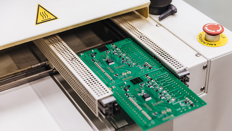
Advanced Fabrication Process
- HDI and Multi-layer PCBs: The design work of modern circuit boards adopts standardized sequential lamination processing technology for multilayer circuit board products with specifications of 8 layers and above, and such sequential lamination processing technology can achieve the high-density interconnection structure design of circuit board traces in various compact hardware layout spaces.
- Special Finishes:Gold immersion (ENIG) for high-reliability boards, organic finishes (OSP) for low-cost PCB builds where shelf-life is less critical.
- Panelization:Multiple boards fabricated in a single panel for efficiency and reduced assembly labor per unit.
PCB Assembly Services and Automation
- Modern PCBA assembly production lines integrate and apply standardized robotic operation technology, industrial-grade Automated Guided Vehicle (AGV) supporting equipment and full-production-process real-time process monitoring technology, and by virtue of the integrated application of various such technologies and equipment, they achieve standardized collaborative operation in all links of production and manufacturing and full-process dynamic process control.
- PCB assembly services are equipped for the full range of production: from prototyping to mass production, and from simple two-layer PCB to advanced multi-layer PCBA.
Quality Control and Environmental Considerations
- SPC (Statistical Process Control):Tightly manages solder paste, placement, and reflow quality.
- Green Practices:Closed-loop chemical recycling, lead-free assembly and minimal scrap—key concerns in today’s electronics manufacturing.
- Batch Traceability:Advanced PCB assembly today can serialize and trace every assembly with barcodes, linking back to lots, operator logs and test results.
Industry Use Cases and Applications
- Consumer Electronics:The distinction between PCB vs. PCBA is everywhere: PCBs in a wireless earbud’s charging case, but PCBA in the earbud itself.
- Medical:From simple diagnostic aids with rigid PCB to flexible, fully assembled multi-layer PCBA for implantables.
- Automotive:Standard PCB for cockpit lighting; fully assembled PCBA for engine and safety modules.
- Power and Industrial Controls:High-current aluminum PCBs for power LEDs; rugged, conform al-coated PCBA in industrial automation.
- IoT Devices:Rely on ultra-compact, rigid-flex multi-layer PCBA for sensors, radios, and embedded controllers, leveraging both sides of the board to maximize real estate in tiny casings.
Manufacturing and Cost Considerations
The Cost of PCBA vs. Bare PCB
The cost of PCBA is considerably higher than that of a bare PCB. Here’s why:
- Material and Fabrication:
Low-cost PCB options are available for simple single- or double-layer boards, but costs rise with multi-layer PCBs, controlled impedance or specialty materials.
- Component Procurement:
Electronic component prices may fluctuate with the global supply chain. Sourcing reliable, authentic parts is a major factor in the total PCB assembly cost.
- Assembly Labor and Overhead:
Automated SMT lines will bring the per-board assembly labor cost down for high volume, whereas bespoke low-run boards might incur a higher per-unit labor bill.
- Testing and QA:
Post-assembly inspection (AOI, ICT, functional testing) is essential for every finished product. More complex assemblies with denser components or high-reliability applications may require additional and more costly testing steps.
- Yield and Rework:
Each error in the PCB assembly process—misplaced components, solder bridges, or poor wetting—impacts the yield, requiring costly rework or even scrapping of the assembly.
Strategies to Reduce Manufacturing and Assembly Costs
- Standardize on common components and PCB stackups where possible.
- Engage early with your PCB manufacturer for Design for Manufacturing.
- Use prototyping to mass production PCB assembly services with scalable logistics, so the transition is seamless as demand grows.
- Where budget is critical, communicate constraints clearly; tradeoffs between lowest unit cost and long-term reliability should be explicit.
Total Cost of Ownership & Risk Management
It’s not just the cost of PCBA or the per-unit PCB that matters. Understanding PCB cost drivers and production risks can help you make superior decisions:
- Supply Chain Diversification:Maintain relationships with multiple PCB assembly services.
- Yield Management:Monitor yield rates at both the fabrication and assembly stages—catch issues early to prevent downstream costs.
- Documentation Control:Ensure every Gerber, BOM, centroid and test file is versioned and accessible—a single error can disrupt production for weeks.
- IP Protection:For sensitive projects, use trusted partners with proven records in IP security, especially when sourcing offshore.
The Evolution of Circuit Boards
Milestones in PCB Development
From the first single-layer PCB prototypes in radios to multi-layer HDI boards embedded in modern smartphones, the journey has been remarkable:
- Transition from paper and Bakelite to modern FR4 and polyimide.
- Invention of plated through holes enabled complex, multi-layer routing, driving miniaturization.
- The move to double-sided and then multi-layer PCBand multi-layer PCBA assemblies was pivotal for high-speed computing and networking.
Sustainable & Green Electronics Manufacturing
Today’s electronics manufacturing prioritizes sustainability:
- Lead-free soldering, RoHS compliance, and closed-loop water processing cut environmental impact.
- Some suppliers now offer recycled copper foil, reclaimed epoxy and advanced material recycling for both PCBs and PCBAs.
Advanced PCB Material Trends
Demand for better signal integrity and thermal dissipation has led to the adoption of:
- High-Tg FR4, ceramic, aluminum-core PCBs.
- PTFE-based high-frequency boards for RF and millimeter-wave systems.
- Hybrid stackups uniting rigid and flex layers for medical, military and aerospace.
Choosing the Right Service for Your Project
When to Choose Bare PCB vs. Assembled PCBA
- Bare PCB:
- Best for prototyping, academic work, DIY electronics or in-house assembly where speed and low cost are paramount.
- PCBA:
- Preferred for end-use, turnkey product or when assembly expertise, test coverage, and production volume scalability are required.
Turnkey PCBA Service: Leverages the assembly provider’s component sourcing, fabrication, rapid prototyping and rigorous testing. Ideal for startups, scaling products, or anyone seeking peace of mind with a fully tested, plug-and-play solution.
Selecting a Good PCB Manufacturer
Evaluating Suppliers
- Insist on seeing example boards—or even better, run a small test batch.
- Demand transparency for lead times, yield rates, and rework policies.
- A good PCB manufacturer should facilitate open communication between your engineers and their process experts.
Onshore vs. Offshore PCB Assembly Services
- Onshore may mean higher cost but is often offset by local expertise, tighter QA and faster turnaround for prototypes.
- Offshore excels at scaling mass production and sourcing odd parts but requires coordination for logistics and communication.
Handling Quality Issues
- Clarify acceptance standards, inspection frequency, and documentation process before issuing a PO.
- When issues arise, use a structured 8D/CAPA approach and request detailed root cause and corrective action plans.
Frequently Asked Questions (FAQ)
What is the primary difference between PCB and PCBA?
A PCB is a bare circuit board—basically, the wiring map—while a PCBA is a PCB that has undergone the assembly process, with components soldered onto the board, becoming a fully functional, testable and deployable electronic device.
What are the key differences between bare PCB and finished PCBA in cost and lead time?
The cost of PCBA is always higher, reflecting assembly labor, component prices and extensive QA. A bare PCB may take a few days to deliver; a full PCBA, especially for complex assemblies, may require several weeks.
Can a multi-layer PCBA be reworked if there’s a problem?
Sometimes, but the risk and cost escalate quickly, especially for high-density multi-layer PCBs with fine-pitch or BGA packages. Proper DFM and early test/inspection coverage minimize the need for such expensive fixes.
What files are required for a turnkey PCBA order?
- Gerber files (circuit board layout)
- BOM (Bill of Materials)
- Centroid/pick-and-place file
- Assembly drawings (if special instructions)
- Test specifications (for in-circuit or functional testing)
What is a “circuit card assembly”?
It’s another term for PCBA: a complete circuit board with all electronic components mounted, tested and ready for use.
Is “PCB assembly process” different for prototyping versus production?
Usually, prototyping uses manual or semi-automated assembly labor for speed and flexibility, while high-volume production leverages fully automatic assembly lines and robust process controls.
Conclusion
Understanding the distinction between PCB and PCBA is vital in all stages of an electronic device lifecycle. The PCB is a bare platform, the physical map over which you realize a circuit design. PCBA is a PCB translated into a fully functioning product by careful assembly and test. Each plays different but necessary roles in electronics manufacturing, influencing cost, speed, quality, and ultimate market success.
From bare PCB into a fully assembled PCBA, every step—from circuit board to complete circuit board—demands attention to detail, thoughtful supplier selection, and a holistic view of your design and manufacturing strategy. Whether you need the lowest-cost PCB for a proof-of-concept or the assurance of a turnkey PCBA for mass production, understanding these critical differences helps you deliver reliable, high-quality electronics faster and with greater confidence.