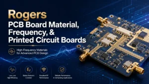
Introduction: Why Telecom PCB Assembly Is the Backbone of Modern Communications
In today’s hyper-connected world, communication systems—ranging from 5G base stations to fiber networks and space-borne satellites—are the circulatory system of our economy and society. Their invisible backbone? Telecom PCB assembly and high-performance pcb assemblies built for the telecom industry.
Telecom PCB assembly is not your average PCB manufacturing job. It is precision assembly designed to support high-frequency signals and maintain signal integrity even in the most demanding telecommunication devices. High-reliability PCBs are what make high-frequency communication, ultra-low signal loss, and mission-critical uptime possible.
Whether it’s a router managing high-speed data transmission, a satellite keeping the globe synchronized, or a cellular base station bridging continents, reliable pcb assembly services for telecom are fundamental for global connectivity and the evolution of the telecommunications industry.
What Is Telecom PCB Assembly?

Telecom PCB assembly refers to the specialized process of fabrication and assembly of printed circuit boards tailored specifically for telecommunication devices, telecommunication equipment, and cutting-edge telecommunication systems.
Unlike standard PCB assembly, which might suffice for consumer electronics, telecom PCB assembly must meet much higher thresholds for performance, reliability, thermal management, and EMI immunity. In this sector, high-reliability PCB assemblies are expected to operate non-stop for years in rugged, demanding environments—powering mission-critical telecom networks and communication devices worldwide.
Key Aspects of Telecom PCB Assembly:
- High frequency and high speed support Telecom infrastructure boards are expected to handle signals well into the GHz range while juggling complex communication protocols, all without introducing significant attenuation or distortion. That means the PCB material, stackup, and routing all have to be carefully chosen to keep losses to a minimum.
- Impedance control and signal integrity – Maintaining consistent impedance across every trace isn’t just a nice to have – it’s a non negotiable requirement for preserving signal accuracy and keeping crosstalk under control. This calls for meticulous layout work, controlled dielectric spacing, and often simulation driven design to verify that the board behaves as predicted before it ever hits production.
- Environmental durability – Telecom gear doesn’t live in a cushy lab environment. It ends up on cell towers, in roadside cabinets, or on rooftops, where temperature swings, humidity, vibration, and power surges are just part of daily life. So the PCB needs to be rugged enough to handle those extremes without compromising performance or long term reliability.
- Meticulous quality control – Every telecom board that leaves the factory has to go through a rigorous suite of quality checks – not just visual or automated optical inspection, but also functional testing under realistic operating conditions. And on top of that, full traceability records are maintained for each board, so if any issue surfaces later, you can track it all the way back to its origin.
The Role of PCB Assemblies in Telematics & Telecom Electronics
Telecommunications equipment today combines traditional communication technologies with tomorrow’s innovations, all enabled by expertly engineered pcb assemblies.
Where Telecom PCB Assemblies Make a Difference
- Core networking and telecom: Telecom PCB assemblies in routers and switches sustain high-speed, high-reliability backbone operations.
- Telematics: Custom PCBs fuse GPS, cellular, Wi-Fi, and CAN for advanced vehicle and asset tracking.
- Satellites and space systems: Only the most robust PCB assemblies are trusted for satellite communication systems and orbital electronics.
- IoT and edge devices: Compact, multilayer telecommunication PCBs drive connectivity in every smart device, from environmental sensors to industrial controllers.
Types of Telecommunication and Communication Systems
Modern telecom networks employ a range of specialized communication systems, all relying on precise PCB assemblies:
| System Type | Example Applications | Special PCB Assembly Needs |
| Two-way speech/transmission systems | Cellular, landlines | Low-noise, high-reliability, EMI-shielded |
| Broadcast communications | TV, public emergency alerts | High-power, thermally managed |
| Data transmission systems | Fiber networks, routers, cloud servers | Controlled impedance, high-speed, multilayer |
| Integrated voice/data (VoIP, PBX) | Unified enterprise communications | Mixed-signal, EMI control |
| Wireless communication systems | Wi-Fi, mobile, IoT nodes | Miniaturized PCBs, flexible/rigid-flex |
| Satellite communication systems | Spaceborne comms, GPS, IoT satellites | Space/thermal resilient, precision assembly |
High-Frequency Telecom & Communication Technologies
Telecom applications increasingly require PCB assemblies that withstand high-frequency telecom environments, such as mmWave 5G, next-gen fiber, and global satellite networks.
Applications: Where Telecom PCB Assemblies Power the World

PCB assemblies are at the heart of every sector in the telecommunications industry. Examples include:
- 5G/4G/3G Base Stations: Robust telecom PCBs ensure low-latency, high-frequency data aggregation and real-time switching.
- Data center routers and backbone switches: Handle high-speed, high-bandwidth transfers.
- Satellite communication systems: Use precise, space-rated PCBs to maintain signal integrity under harsh cosmic conditions.
- IoT platforms and gateways: Small-form, high-density assemblies for constant connectivity and control.
- Industrial telematics: Custom PCB assemblies for vehicle diagnostics, asset security, and smart fleet management.
- Emergency communication systems: Rugged, redundant circuit boards ensure communication when every second counts.
Specialized Assembly for Telecom Applications
PCB assembly for telecom also enables multimedia streaming, medical telemetry, defense communications, and public safety—environments where reliability in telecom networks is non-negotiable.
Telecom PCB Materials, Board Types, and Custom Solutions
Choosing the Right Materials
The performance of telecom pcbs hinges on advanced materials:
- Rogers, PTFE, and Low-loss FR-4: Support high-frequency signals, maintain impedance stability, and reduce signal loss.
- Polyimide and Metal Core: Maximize heat dissipation for base stations and outdoor routers.
- Flexible and Rigid-Flex Structures: Allow miniaturization for IoT, wearables, and aerospace telecom devices.
| Material Type | Advantage for Telecom Assembly | Common Applications |
| Rogers/PTFE | Minimal signal loss, precise impedance | Satellite, mmWave, 5G RF boards |
| Low-loss FR-4 | Robust, affordable | Data networks, VoIP, industrial comms |
| Polyimide | Flexibility, temperature resistance | Automotive, aerospace, ruggedized assemblies |
| Metal Core | Efficient thermal management | High-power base stations, RF amplifiers |
Custom PCB Solutions
Telecom PCB assembly services deliver custom PCB assemblies that fit exactly into your system’s needs—whether for unique form factors, frequencies, or environmental requirements.
The Complete Telecom PCB Assembly Process
The telecom PCB assembly process is highly structured and exacting. Here’s how the best in the business deliver outstanding results:
Step-by-Step Telecom PCB Assembly Techniques:
- Pre-fabrication PCB Design Review: Ensuring that layout, impedance, and material choices align with telecom system demands.
- Prototype Production and Validation: Building and testing early batches to identify signal integrity, EMI, or routing issues before scaling.
- Automated Assembly: SMT for miniaturized, high-density boards; through-hole for robust connectors and power circuitry; and mixed-technology where required.
- Reflow Soldering and Wave Soldering: Reliable joints for both micro-BGAs and high-power telecom components.
- Automated Optical Inspection (AOI) & X-ray Testing: Catching microscopic and hidden assembly flaws in complex PCB assemblies.
- Functional Testing: Full system emulation to assess performance under network protocol loads, validating reliability and correct high-frequency communication.
- Final Assembly, Conformal Coating, and Traceability: Protects finished assemblies and ensures every board is fully documented and certified for telecom use.
Precision Assembly for Signal Integrity and EMI Control
Maintaining signal integrity is the holy grail of telecom PCB assembly. Here are the top assembly solutions for this goal:
- Controlled Impedance Routing: Ensures consistent, predictable signal travel for high-speed lanes, reducing distortion and signal loss.
- Differential Pair Layouts: Critical for USB, Ethernet, and RF lines to minimize crosstalk and maximize performance in high-frequency communication systems.
- Strategic Ground Planes and Shielding: Prevent electromagnetic interference (EMI) from disrupting sensitive high-frequency telecom signals.
- Thermal Pathways: Efficient thermal vias, heavy copper pours, and, when required, integrated metal cores in pcbs help maintain reliability for high-power telecom equipment such as base stations and outdoor routers.
Telecom PCB Assemblies: Capabilities and Specialized Services
Leading PCB assembly services for telecom go beyond just building assemblies—they integrate into your product’s entire lifecycle.
Telecom PCB Assembly Capabilities:
- End-to-end PCB assembly service: Covering everything from prototype to mass production.
- Versatile assembly techniques: Experts in SMT, through-hole, mixed-technology, and high-density PCB assembly for telecom.
- Tailored PCB manufacturing for telecom applications: Whether you need flexible, rigid-flex, metal core, or high-layer-count boards.
- Comprehensive functional testing: Ensures every circuit board and PCB assembly delivers in real-world telecom networks.
- Stringent documentation and traceability: Support regulatory audits, recalls, and continuous product improvement.
Specialized Assembly Services for Telecom:
- Rapid prototyping of telecom pcbs and assemblies for fast-paced R&D projects.
- Controlled environmental testing for outdoor telecom devices or high-frequency telecom systems exposed to challenging conditions.
- Component lifecycle management: Ensures consistent sourcing and supply chain stability for long-term reliability and serviceability.
Measuring Success: Metrics and Field Reliability
Reliability in telecom is more than a buzzword—it’s a requirement. High-reliability PCB assemblies ensure near-zero outages and minimal downtime, which translates into:
- High uptime (99.999% or ‘five nines’ reliability) for telecom equipment
- Low field failure rates: The benchmark in telecom is fewer than 100 ppm (parts per million) failures over a board’s lifecycle.
- Signal integrity and low signal loss: Assured by up-front design, stringent assembly techniques, and ongoing functional testing.
- Robust field performance: Boards must pass humidity, thermal cycling, vibration, and electrical surge tests that mirror real telecom applications.
Critical Design and Fabrication Tips for Telecom PCB Assembly
The secret to world-class telecom PCB assembly? Smart design choices, early validation, and specialized fabrication and assembly.
Top Tips:
- Co-design with your assembly partner: Involve your assembler at the design phase for valuable feedback on stack-up, routing, and test access.
- Prioritize signal integrity and impedance control over raw board density.
- Choose the right surface finish: ENIG for signal paths, hard gold for high-insertion connectors.
- Design for testability (DFT): Add extra test points for functional and in-circuit checks.
- Specify the correct materials: Don’t cut corners with standard FR-4 on high-frequency or high-speed telecom projects; only use certified telecom PCB manufacturers.
- Document every step: From layout to fabrication and assembly, create a traceable record for compliance.
Comprehensive Telecom PCB Assembly Services from LHD TECH
If your telecom projects demand zero compromises, partnering with a dedicated telecom PCB manufacturer is critical.
LHD TECH provides:
- High-frequency, high-speed data transmission PCB assemblies—engineered specifically for telecom networks and communication devices.
- Full-lifecycle assembly services for telecom: from DFM and prototyping to final assembly, functional testing, and global rollout.
- Unmatched quality control with ISO certification, IPC-A-610 Class 3 workmanship, and complete batch traceability.
What Sets Telecom PCB Assembly Apart from Standard PCB Assembly?
| Feature | Telecom PCB Assembly | Standard PCB Assembly |
| Frequency/Speed | Handles high-frequency, high-speed signals | Suitable for lower-frequency signals |
| Materials | Rogers, PTFE, low-loss laminates | Mostly standard FR-4 |
| Signal Integrity | Advanced impedance, EMI shielding, signal loss prevention | Basic design controls |
| Quality Control | Enhanced (ISO, functional testing, AOI, X-ray) | Basic inspection/testing |
| Reliability Requirements | 24/7, harsh conditions, long field life | 2–5 years, consumer-grade |
| Assembly Techniques | SMT, through-hole, mixed-technology, custom | Mostly SMT or TH only |
| Documentation & Traceability | Full regulatory, telecom-focused | General, less stringent |
| Use Case | Telecom, networking, satellite, datacenter | Consumer, general industrial |
Telecom PCB assemblies always prioritize telecom-specific needs for mission-critical operations, signal integrity, and field reliability.
Industry Challenges and Best Practices in High-Speed, High-Frequency PCB Assembly
Key Challenges:
- High-frequency design complexity: Requires expertise in layout, simulation, and controlled impedance.
- Component miniaturization: Demanding HDI and advanced mixed-signal assembly.
- Thermal stress and environmental exposure: Critical for base stations, satellite links, and networking infrastructure.
- Material cost and sourcing: High-quality laminates, rigid-flex, and specialty components come at a premium.
Best Practices:
- Employ advanced CAD tools for simulation before fabrication and assembly.
- Prototype and validate with functional testing under actual telecom loading scenarios.
- Build close relationships with trusted PCB manufacturers and assembly partners familiar with the telecommunications industry.
- Never overlook the value of redundant design and extensive testing for field readiness.
Quality Control, Compliance, and Lifecycle Assurance
Ensuring the quality of your telecom PCB assembly isn’t a single step—it’s an ongoing discipline.
- ISO, CE, and FCC compliance: Every telecom PCB must pass regional and international benchmarks.
- IPC-A-610 Class 3 quality control: The “gold standard” for high-reliability PCB assembly in telecom and networking.
- Environmental and lifecycle testing: Simulate years of field use before launch to predict—and prevent—failures.
- Documentation and traceability: Every finished circuit board batch is recorded for audits, warranty, and future upgrades.
FAQs About Telecom PCB Assembly
1. What does PCB assembly do in telecom equipment?
PCB assembly mounts and connects electronic components onto a printed circuit board, creating functional circuits for routers, base stations, switches, gateways, RF modules, and other telecom equipment.
2. What is the difference between a PCB and a PCB assembly?
A PCB is the bare printed circuit board without components. A PCB assembly (PCBA) is a PCB populated with components through SMT, through-hole, or mixed assembly processes.
3. How much does telecom PCB assembly cost?
The cost depends on board complexity, component count, quantity, assembly technology, testing requirements, and component sourcing. High-frequency or high-density telecom assemblies may require additional process control and testing.
4. How long does telecom PCB assembly take?
Lead time depends on PCB complexity, component availability, quantity, and testing requirements. Prototype telecom PCB assemblies can often be completed faster when components and manufacturing files are ready.
5. What testing methods are used for telecom PCB assemblies?
Common methods include AOI, SPI, X-ray inspection, ICT, flying probe testing, functional testing, and electrical testing. The appropriate combination depends on the telecom product and reliability requirements.
6. What PCB materials are commonly used for telecom equipment?
FR-4 is widely used for standard telecom circuits, while Rogers and other high-frequency laminates are used for RF, microwave, antenna, and low-loss signal applications.
7. What are common problems in telecom PCB assembly?
Common issues include solder defects, component misalignment, BGA voids, impedance deviations, signal integrity problems, contamination, and thermal management issues.
8. Why do telecom PCB assemblies fail?
Failures can result from poor solder joints, excessive heat, vibration, moisture, component defects, incorrect impedance, PCB design issues, or inadequate manufacturing process control.
9. Can a telecom PCB assembly be repaired?
Yes. Many telecom PCB assemblies can be repaired by replacing damaged components or correcting solder defects. However, repair feasibility depends on component type, board damage, and reliability requirements.
10. What affects the cost of a telecom PCB assembly?
Major cost factors include PCB layer count, board size, component quantity, BGA and fine-pitch devices, RF materials, assembly volume, testing, conformal coating, and other special process requirements.
How to Choose the Right Telecom PCB Assembly Partner
When it’s time to select a vendor, look for:
- Telecom-focused experience: Not every PCB assembler understands the intricacies of telecommunication devices or high-frequency challenges.
- End-to-end capabilities: From DFM and prototype to full-scale, traceable final assembly.
- Transparent compliance: ISO, IPC, RoHS, CE, and FCC as baseline credentials.
- Field-proven results: Ask for telecom project references and tested pcb assembly solutions.
Innovation and the Future of Telecom PCB Assembly
As telecom and networking evolve—6G, AI-driven networks, and edge computing—the demands on telecom PCBs will continue to grow:
- Smart PCB assemblies that provide self-diagnosis for proactive maintenance.
- Even higher frequencies handled with precision thanks to new laminates and 3D PCB fabrication.
- Green, sustainable PCB manufacturing using recyclable materials and eco-friendly practices to support global telecom expansion.
From Prototype to Field—Supporting Your Telecom Projects
Telecom PCB assembly is no longer a commodity—it’s your network’s strategic edge.
- Start every project with expert DFM and prototype validation.
- Optimize assembly for signal integrity, impedance, and thermal management before the first mass run.
- Partner with a telecom PCB manufacturer that offers full-lifecycle support, advanced quality control, and a relentless focus on reliability.
Conclusion: Building the Future of Telecom and Networking with Advanced PCB Assembly Solutions
The world’s fastest, most reliable, and innovative networks rely on advanced telecom PCB assembly. From custom telecommunication PCB assembly to complex, high-frequency telecom systems and satellites, the right approach means greater uptime, safer operations, and new capabilities for tomorrow’s telecom products.
In the hugely competitive telecommunications industry, every detail matters. The move to 5G and soon 6G, the expansion of satellite communication systems, and ongoing growth in broadband demand all raise the stakes for pcb assembly for telecom. Only partners with proven expertise in telecom PCB assembly, precision assembly, and robust quality control can reliably deliver the performance, compliance, and reliability in telecom expected by today’s customers and regulatory authorities.
The Path Forward
- Leverage innovation: Integrate high-frequency, high-speed and custom PCB assembly techniques to future-proof your networks.
- Insist on collaborative assembly services for telecom: Your best outcomes will come from close, proactive engagement between your design and manufacturing teams from the first prototype to every deployed circuit board.
- Prioritize supply chain and compliance: Choose PCB manufacturers who can assure traceability, batch-level records, and full lifecycle support for every stage of the final assembly process.
- Commit to meticulous quality and testing: Make thorough functional testing and documentation a foundation of every deployment, from core routers to IoT endpoints and satellite comms.
Final Takeaway
Telecom PCB assembly services are the unseen engine of the world’s digital communications. From the billions of telecommunication devices keeping people connected, to the telecom PCBs powering 24/7 backbone networks, the right approach to design, fabrication, assembly, and testing enables the reliability, clarity, and speed we all take for granted.
Every signal, every byte, every call and connection—across continents or to space—ultimately depends on the expertise and rigor behind your telecom printed circuit boards. Now is the time to invest in advanced, customized, and reliable PCB assemblies to support the unstoppable future of telecommunications.