Introduction: Why PCB Cost Matters
Whether designing a hobbyist project or developing the next consumer breakthrough, understanding PCB cost is essential. For decades, designers and procurement specialists have been faced with one persistent question: How much does a custom PCB cost, and what can I do to manage it? The right approach to circuit board pricing can mean the difference between a successful product launch and budget disaster.
Today’s electronics are built on a foundation of printed circuit boards (PCBs)—from single-layer prototypes to multi-layer, high-density commercial boards. The range of custom circuit board cost can be huge: a simple FR-4, 2-layer PCB might be less than $2 per board at volume, whereas high-performance, complex designs for RF or medical use can exceed $500 each. Making the right decisions on pcb materials, layer count, and PCB design will help you optimize both cost and performance.
Understanding the Factors That Affect Custom Circuit Board Cost
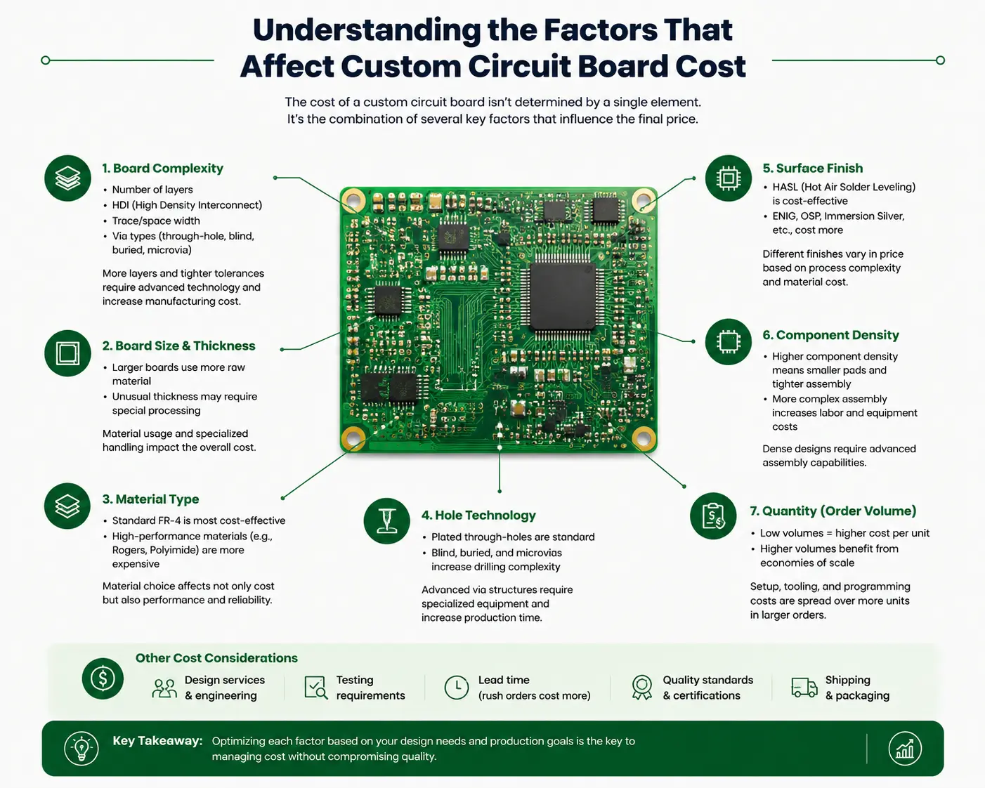
The final cost for your custom PCB or custom printed circuit board comes from a blend of technical requirements and manufacturing economics. Custom circuit board cost is never determined by a single factor. Instead, smart buyers look at the following:
Key Variables That Define Overall Cost
- PCB Materials: From cost-effective FR-4 to high-performance materials like Rogers or metal core substrates, your dielectric and copper choices matter.
- Number of Layers: More layers mean more fabrication steps, increased material, specialized processes, and often more expensive to produce.
- Board Size: Both the overall footprint and how it fits on the manufacturer’s production panel.
- PCB Design Complexity: Vias, trace width, controlled impedance, BGA footprints, and split planes all affect costs.
- Surface Finish & Solder Mask: ENIG, HASL, OSP, and even non-standard solder mask colors alter both board prices and production times.
- Order Quantity: The cost per unit drops dramatically as you mass-produce or batch order multiple boards.
- Lead Time: Expedited orders increase the overall cost as they “jump the queue” in production.
- Testing & Quality Control: Prototypes may skip some steps, but production PCBs destined for regulated markets (medical, automotive, aerospace) incur additional costs.
- Assembly & Components: If you’re ordering assembled PCBs, BOM, stencil, component sourcing, and reflow steps all add to your final cost.
Major PCB Cost Factors
| Factor | Low-Cost Option | Premium/High-Requirement Option |
| PCB material cost | FR-4, epoxy | Rogers, polyimide, metal core |
| Layers | 1-2 layers | 4-layer, 6-layer, 8-layer |
| Size | Small (50x50mm) | Large/custom/mechanical cutouts |
| PCB complexity cost | Wide traces, wide spacing | Fine pitch, HDI, BGA, microvias |
| Finish | HASL | ENIG/gold/immersion silver/tin |
| Quantity | 1000+ (“mass production”) | 1–10 (prototype/small batch) |
| Testing/QA | AOI/electrical only | X-ray, ICT, full traceability |
Navigating PCB Materials and Their Cost Impact
When designing a PCB, selecting the right pcb materials is your first opportunity for savings or increased functionality. Most commercial PCBs use FR-4 (fiberglass-reinforced epoxy), but some printed circuit applications require specialized materials for high signal integrity or power performance.
Standard and High-Performance PCB Materials
- FR-4: The world’s most common PCB substrate, balancing performance and low cost.
- High-Tg FR4: Improved thermal stability for lead-free solder or high-temperature applications.
- Materials Like Rogers/PTFE: Used in RF or high-frequency designs due to their low Dk (dielectric constant) and low loss, but they require more materials and cost more.
- Polyimide: Used for flex PCBs and applications demanding thermal cycling endurance.
- Metal Core (MCPCB): For power electronics, LEDs, or applications needing improved heat dissipation.
PCB Materials Table—Performance & Cost
| Material | Typical Applications | Signal Integrity | Relative Cost vs FR-4 |
| FR4 | Consumer electronics, prototypes | Good | 1x (baseline) |
| High Tg FR-4 | Automotive, industrial, high-temp | Good+ | 1.3x |
| Rogers/PTFE | RF/wireless, antennas | Excellent | 4x–8x |
| Polyimide | Flexible PCBs | Good | 5x |
| Metal Core | High-power lighting, LEDs | Fair/Grounded | 2-3x |
Layers, Size, and PCB Design Complexity
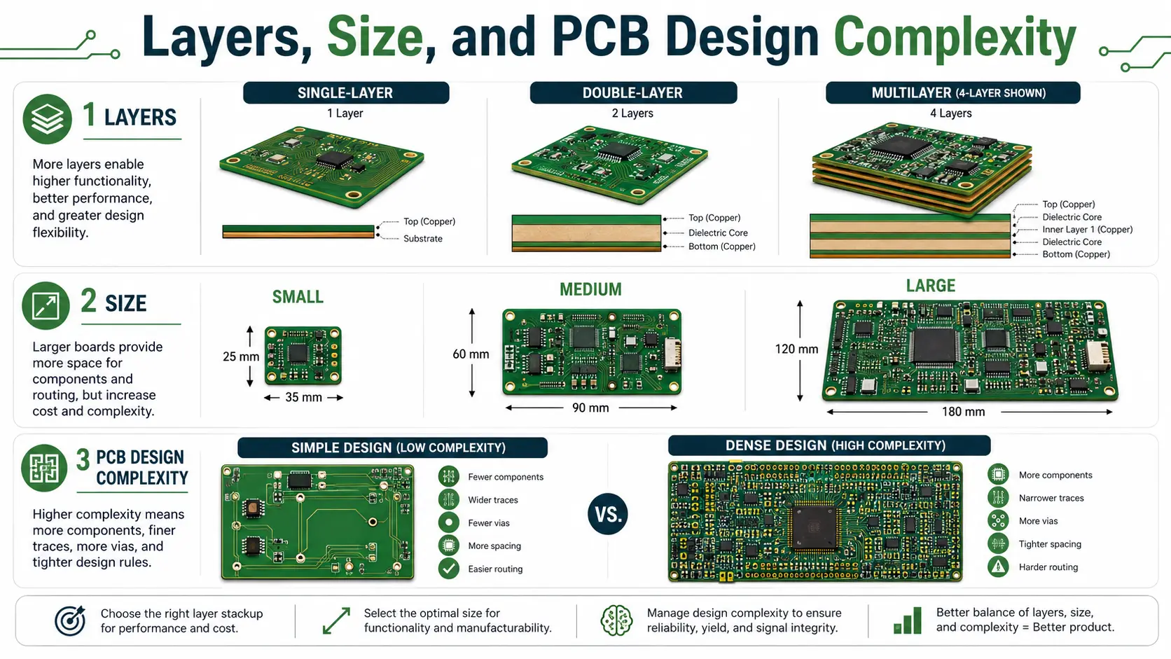
One of the factors that affect custom circuit board cost most significantly is the combination of layer count (number of layers), board size, and pcb design complexity. Each variable multiplies both material and process costs.
PCB Layer Count and Stack-Up
- 2 Layers: Standard for simple or double-sided designs; most cost-effective for prototypes and many small devices.
- 4-Layer and Above: Used for complex routing, signal/power plane separation, better EMI, or compact form factors.
- Additional Layers: Boards with 6, 8, or 12+ layers support complex, dense circuitry (e.g., servers, telecom, advanced IoT) but take longer to manufacture and are expensive to produce.
Board Size and Panel Utilization
- Board size impacts how many units fit onto a manufacturer’s panel. Fewer units per panel mean a higher share of setup and waste per board.
- Panel Optimization: Modern PCB suppliers use CAD algorithms to fit multiple boards on a panel for best yield.
- Complex Designs: Odd shapes, large cutouts, or unorthodox thicknesses all increase material waste and board prices.
Trace Width & Vias
When designing a PCB, trace width and via strategy significantly impact both manufacturing complexity and final pricing. Narrow traces, which are necessary for dense or high-frequency circuits, require more precise fabrication and inspection, raising the pcb cost. Standard traces (such as 6/6 mil) are much more cost-effective than ultra-fine traces (2/2 mil).
Vias allow electrical connections between layers in your PCB stack-up. There are several types:
- Through-hole vias: Standard and lowest cost, connect all layers.
- Blind/Buried vias: Only connect certain layers; typically cost 30–80% more due to extra drilling and process steps.
- Microvias: Used in HDI PCBs for high-density applications (like smartphones and wearables); these take advanced laser drilling and can cost per board up to 200% more than using only through-holes.
- Via-in-Pad: Primarily for BGA footprints; expensive to produce but sometimes unavoidable for ultra-compact layouts.
Surface Finishes, Solder Mask, and Via Technology
The surface finish not only protects copper during storage and soldering, but also impacts assembly quality and long-term field reliability.
Common PCB Finishes & Their Price Impact
- HASL (Hot Air Solder Leveling): Baseline, lowest pcb prices, good for most prototypes and production runs using through-hole or coarser pitch SMD components.
- OSP (Organic Solderability Preservative): Also low-cost, ideal for high-volume SMT with rapid assembly cycles, but with shorter shelf life.
- ENIG (Electroless Nickel Immersion Gold): Prized for flatness and oxidation resistance, critical for BGA, fine-pitch SMT, and wire bond areas. Raises pcb cost per square inch by 80%–150% over HASL.
- Hard Gold/Selective Gold: Only apply where durability is essential—such as edge connectors—because of the very high cost.
- Immersion Silver/Tin: Chosen for specific high-frequency or contact-reliability needs.
Solder Mask
- Standard green solder mask is most cost-effective and offers high reliability.
- Custom colors (white, black, red, blue) can increase fabrication complexity and cost per board.
PCB Finishes, Example Board Prices
| Finish Type | Small Batch Unit Price | Volume Unit Price | Best Use |
| HASL | $2–$5 | <$1 | General, prototypes |
| OSP | $3–$6 | $0.80–$1.25 | High-volume SMT, quick use |
| ENIG | $8–$20 | $2–$6 | HDI, BGA, high-end boards |
| Hard Gold | $18+ | $8+ | Wear-prone connectors |
Manufacturing, Assembly, and Production Process Cost Drivers
The PCB Manufacturing Process
The fabrication of a modern PCB involves several steps: imaging the circuit from your Gerber files, drilling, copper plating, etching, solder mask application, surface finish, legend printing, routing, and inspection. Each adds incremental pcb manufacturing cost, especially for complex or high-reliability designs.
- Drilling: More holes, smaller diameters, or tighter tolerances (especially on HDI or BGA boards) drive up process time and wear on drill bits.
- Impedance Control: Requires specialized test coupons, controlled materials, and tight stack-up management, increasing production process cost.
- Heavy Copper: For power or LED circuits, adds copper foil outlay and requires extra plating time.
PCB Assembly & PCBA Cost Factors
- Solder Paste and Reflow: Boards with only single-side component placement are much quicker and less costly to assemble than double-sided.
- Stencil: Required for accurate solder paste application in SMT lines; size and complexity affect individual stencil cost (often $30–$120).
- Component Sourcing: Including resistor, capacitor, ICs, and all electronic components from a BOM, can be a major part of overall cost, especially during supply shortages or for legacy/obsolete parts.
- BGA, QFN, and Fine Pitch: More expensive to assemble and require AOI/X-ray for quality assurance.
Testing, Quality Control, and Hidden Costs
PCB Testing & Quality Control (QA/QC)
- Electrical Test: Most PCBs are 100% electrically tested today, even for low prices. However, for large panels or fine-pitch layouts, some manufacturers charge extra.
- AOI (Automated Optical Inspection): Used post-fabrication and post-assembly for solder joint inspection.
- ICT/In-circuit Test & X-ray: Required for dense or high-reliability boards, especially with BGA or hidden solder joints.
- Traceability: Medical, aerospace, and automotive boards require documentation and lot traceability, raising the final cost.
- Setup (NRE) & Tooling: One-off fees for programming test equipment, electrical fixtures, and sometimes for custom handling or packaging.
Other Hidden Costs
- Shipping: Fast, tracked delivery can be free with prototypes, but usually adds $10–$40 per order for heavy or expedited shipments.
- Certifications: UL, CE, RoHS, REACH compliance adds documentation and process overhead.
- Packaging: ESD, anti-tarnish, or foam-in-box options protect PCBs but raise costs.
Hidden PCB/PCBA Production Costs
| Category | Typical Range |
| NRE/Engineering | $0–$300+ |
| Stencil | $20–$120 |
| Test Fixture | $150–$1500 |
| ESD/Custom Pack | $0.10–$2/board |
Flexible and Rigid-Flex PCBs: Understanding Cost Premiums
Flexible PCBs
- Materials: Polyimide or PET for base; much more expensive than rigid FR-4.
- Custom PCB Cost: A custom circuit made on flex or rigid-flex can cost up to 10x a basic rigid PCB at low volume.
- Coverlay: Polyimide films replace standard solder mask, adding a durability and price premium.
- Use Cases: Medical sensors, aerospace, wearables, bend-to-fit devices.
Rigid-Flex PCBs
- Stack-up: Mixes rigid FR-4 and polyimide sections in one board. Requires special “bond ply” and hot-press cycles.
- Manufacturing Yield: Extra steps apply stress; yield losses are higher, causing board prices to spike.
- Typical Application: Smart devices, aerospace, medical imaging.
Typical PCB Prices by Type and Volume
| Type/Spec | Prototype (1–10) | 100 pcs | 1,000 pcs (Mass Production) |
| 2-layer FR-4 | $5–$10 | $1.00 | $0.50 |
| 4-layer FR-4 | $10–$20 | $3–$6 | $1.20–$2 |
| 4-layer Rogers | $45–$90 | $32 | $15 |
| 6–8 layer, HDI, BGA | $40–$120 | $18 | $6–$10 |
| Rigid-flex, Polyimide | $60–$180 | $35 | $15–$40 |
Prototype board prices are always much higher per square inch than in mass production.
Practical Strategies to Reduce the Cost of Your Next Project
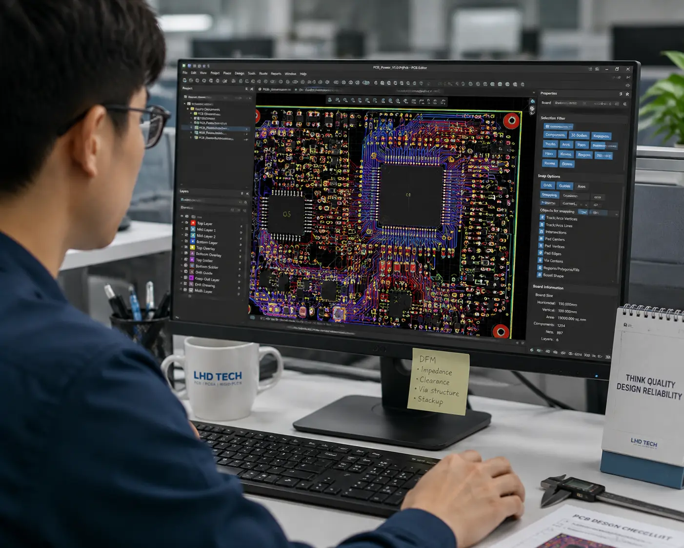
- Minimize PCB Layers: Optimize your schematic and pcb design to achieve signal integrity and routing without unnecessary additional layers. Fewer layers mean lower cost, both in materials and process steps.
- Standardize on Materials: Choose standard FR-4 for most applications. Consider materials like Rogers only where required by RF or high-speed signal designs, as these specialized materials are much more expensive.
- Use Efficient Panelization: Design your pcb board to maximize panel utilization. A smaller board size and common aspect ratio often allow more multiple boards on the panel, which means a lower cost per unit and lower waste.
- Stick to Standard Stack-Ups and Thickness: Unless you have specific requirements, default to 1.6 mm thick boards with standard copper weights. Custom thickness, heavy copper, or exotic stack-ups drive up price and usually extend lead time.
- Control Trace Width & Spacing: Trace width as per IPC guidelines (like 6/6 mil) is less expensive and has better manufacturing yield compared to ultra-fine lines (<4/4 mil), which require tighter process control and advanced capability.
- Limit Complex Vias: Use standard through-hole vias unless you’re designing for HDI or BGA with clear need for blind/buried/microvias. Complex designs, via-in-pad, or large via counts increase both fabrication and AOI/X-ray inspection costs.
- Choose Cost-Effective Finishes and Solder Mask: Use HASL (especially for prototypes or general purpose boards) or OSP if your circuit components will be assembled quickly. Choose green solder mask for best pcb supplier pricing.
- Relax Tolerances When Possible: Avoid over-specifying dimensions, holes, or controlled impedance unless essential for function. Tighter tolerances or impedance-controlled traces require more process control and testing, raising costs.
- Consolidate Orders: If you can, order a larger batch (even delaying a project by a week or two to combine prototypes). Greater volume reduces the impact of setup/NRE charges and achieves low prices.
- DFM: Design for Manufacturability: Consult your pcb manufacturer for DFM feedback early. Small layout, via, or assembly changes often create significant savings. Many board houses provide free DFM checks with your Gerber review.
Advanced Cost-Saving Tips & Real Case Studies
Case Study: Consumer Drone Electronics
Challenge: The original drone design specified a 6-layer HDI PCB with via-in-pad for BGA chips, requiring ENIG finish and blue solder mask for both appearance and technical reasons.
Solution: After a DFM review, engineers reworked the power and signal routing, eliminating two layers, switching to standard green solder mask and HASL finish where possible, and using traditional through-hole vias. The BGA area was minimized.
- Savings:$9.80 to $3.40 per board at 1,000-unit production volume; assembly yield improved by 4% as measured by AOI and X-ray.
Case Study: IoT Prototype Startup
Problem: Their custom PCBs—four-layer FR-4, modest size but with complex cutouts and a white solder mask—were quoted at over $60 each for the first 10 units.
Adjustments: Redesigned for rectangular outline, opted for green mask, and combined three product prototypes onto a single large panel to maximize area usage.
- Savings: Each board cost dropped to $17, and their supplier batch-shipped all 10 prototypes as a single lot, reducing lead time as well.
Why Your Choice of PCB Manufacturer Makes a Difference
A good pcb manufacturer not only delivers high quality standards and reliability but also helps ensure you get a cost-effective solution tailored to your needs.
- Advice: Reputable suppliers offer DFM, prompt support, and will clarify fabrication options to fit every budget.
- Global Experience: The best pcb suppliers operate worldwide, have stellar traceability, and can mass-produce or build low-run prototypes.
- Innovation: Partners who invest in technology provide lower prices by boosting yield and process automation—not by cutting quality.
Conclusion: Mastering PCB Cost for Your Next Project
By understanding the factors that affect every stage of your design, fabrication, and assembly process, you can proactively optimize your project for cost, quality, and lead time. Study your options, engage your manufacturer early, and make design choices that deliver the function you need without over-engineering. Whether you need one prototype or prepare to mass-produce thousands of PCBs, these principles apply:
- Know your stack-up and its impact on overall cost
- Use standard, cost-effective materials unless function dictates otherwise
- Keep your pcb designs as simple as possible
- Leverage pooling, batching, and larger orders when appropriate
Above all, treat your PCB manufacturer as a collaborative partner—they’ll help you reduce risk and maximize value over your entire product lifecycle.
Frequently Asked Questions About Custom Circuit Board Cost
1. How much does a custom circuit board cost?
The cost depends on the board size, layer count, material, quantity, surface finish, and manufacturing complexity. A standard two-layer prototype may cost only a few dollars per board, while complex multilayer, HDI, or high-frequency boards can cost significantly more.
2. How much does it cost to get a custom circuit board made?
A small prototype order commonly costs tens of dollars before shipping, depending on the specifications and quantity. For larger production volumes, setup costs are spread across more boards, reducing the unit price.
3. How much does it cost to design a PCB?
Professional PCB design may cost several hundred to several thousand dollars, depending on circuit complexity, component count, layer count, signal requirements, and the number of revisions. Providing complete schematics and design requirements can reduce engineering time and cost.
4. How much does a two-layer PCB cost?
A small two-layer FR-4 PCB with standard copper thickness, basic design rules, and HASL finish is one of the most economical options. Larger dimensions, thicker copper, ENIG finish, controlled impedance, and tighter tolerances will increase the price.
5. How expensive is it to print a PCB?
PCB fabrication is relatively inexpensive for standard designs, but small prototype orders have a higher cost per board because of setup and processing expenses. Ordering larger quantities usually lowers the unit cost substantially.
6. What is the cheapest PCB material?
Standard FR-4 is usually the most cost-effective material for general-purpose custom circuit boards. CEM-1 may be cheaper for simple single-sided boards, but it has more limited electrical, thermal, and mechanical performance.
7. Why are some PCBs so cheap?
Low-cost PCBs are typically produced with standard materials, common board thicknesses, relaxed design rules, automated equipment, and efficient panelization. Prices increase when a design requires special materials, blind vias, heavy copper, impedance control, or advanced testing.
8. Is it cheaper to make my own circuit board?
Making a simple circuit board at home may be practical for a basic one-off project. However, professional PCB manufacturing is usually more economical and reliable once the costs of tools, chemicals, drilling, plating, testing, and possible rework are considered.
9. How hard is it to make a custom PCB?
Standard single-layer and two-layer PCBs are relatively straightforward to manufacture. Fine-pitch components, HDI structures, blind or buried vias, high-frequency materials, and tight impedance requirements increase both manufacturing difficulty and cost.
10. How can I get an accurate custom PCB cost estimate?
Provide complete Gerber or ODB++ files, drill files, board dimensions, layer count, material, copper thickness, surface finish, quantity, testing requirements, and delivery schedule. Complete manufacturing data allows the supplier to calculate the price accurately and avoid unexpected charges.