Introduction to Printed Circuit Boards
Printed Circuit Board (PCB) is the core supporting platform required for the normal operation of various electronic devices at present. When people use common electronic devices such as smartphones, laptops, remote controls and electronic watches, they are actually interacting with Printed Circuit Boards (PCBs). A Printed Circuit Board undertakes two core functions: the copper circuit layers etched on the insulating substrate are responsible for connecting various electronic components, and the entire board body provides sturdy physical support for all electronic components. This technical carrier has been widely applied in all fields of human life. Whether it is simple-structured children’s toys, precision and complex medical diagnostic equipment, or aerospace technology devices driving cutting-edge exploration, modern Printed Circuit Boards have always been the core power source for various electronic devices to realize their functions.
Printed Wiring Boards: More Than Just Connections
Historically called “printed wiring boards,” PCBs have grown from simple single-layer boards to multi-layer, 3D printed and flexible PCB designs that enable unparalleled complexity and miniaturization in circuit board design.
History and Importance in Modern Electronics
How Printed Circuit Boards Are Used
PCBs evolved from point-to-point wiring—manual connections of each wire and part—which was slow, error-prone and limited. Today’s PCBs set the industry standard for electronic circuit connections and design integrity.
- Printed circuit boards are used in consumer gadgets, industrial automation, avionics, automotive electronics, medical devices and renewable energy systems.
- Advanced printed circuit board manufacturing processes and design innovations drive multidimensional progress in electronic circuits. These technological advancements enable electronic devices to achieve highly compact internal structures, support high-speed and stable signal transmission, ensure long-term operational reliability of complex systems, and effectively control overall costs through mass production methods.
Why PCBs Are the Backbone of Modern Electronics
- Scalable manufacturing:PCB manufacturers use automated tools, meaning even complex, large and layer-board assemblies can be produced quickly and with consistent quality.
- Miniaturization:The entire design of smartphones, wearables and IoT devices is possible due to advanced PCB design.
- Reliability:Rigid PCB designs withstand temperature swings, vibrations and mechanical stress, making them suitable for the harshest environments.
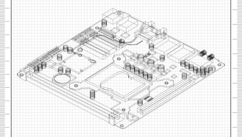
PCB Components and Materials Used
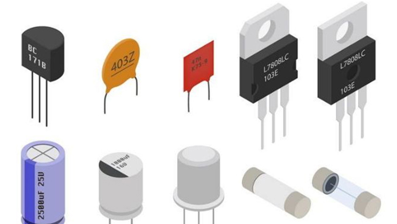
A well-designed printed circuit board balances signal integrity, mechanical support and cost. Every PCB consists of multiple functional layers and materials, each supporting the requirements of the circuit and physical design of the board.
Primary PCB Components
- Integrated circuits (ICs):At the heart of modern electronics, they handle everything from logic operations to signal amplification.
- Active components:Transistors, diodes, crystal oscillators—responsible for switching and processing signals.
- Passive components:Resistors, capacitors, inductors—manage current, store energy and stabilize circuit behavior.
- Connectors, relays, transformers and sensors are critical components. They collectively expand the functional limitations of a PCB in both physical space and electrical performance, establishing stable and efficient signal and power transmission interfaces with external systems.
Materials Used in PCB Design
| Component | Typical Material Used | Function |
| Board substrate | FR4 (fiberglass epoxy), Polyimide, Ceramic, Metal-core | Structural base, insulates electrical layers |
| Copper Layer | Pure Copper, sometimes Silver-plated | Conductive circuitry (“traces,” “planes”) |
| Solder Mask | Epoxy resin (green, red, black) | Protects copper, prevents solder bridging |
| Silkscreen | Non-conductive ink | Printed markings for assembly and repair |
Basics of PCB Design and Board Design Process
Engaging in circuit board design requires first systematically mastering the fundamental design knowledge of printed circuit boards. Designers must fully comprehend the functional requirements and performance specifications of the target circuit. From a single prototype board used solely for concept validation to mature circuit board assemblies ready for direct factory mass production, different types of products adhere to the same fundamental principles during the design phase.
The PCB Design Process – Step by Step
Intro to PCB Design:
- Define circuit requirements: voltage, current, speed, size and environment.
- Gather all electronic components and integrated circuits for your project.
Schematic Creation:
- Engineers must use professional tools to create digital circuit schematics. They utilize software including Altium Designer, Eagle and KiCad to build the logical models of circuits. The finally generated schematics comply with a set of standardized graphical representation specifications, which fully defines the electrical connection relationships of all components in the circuit and clearly demonstrates the specific paths of signal transmission.
- Assign designators and develop a netlist—critical data that guides trace routing.
Board Shape and Layout:
- Determining the physical outline of the circuit board serves as a fundamental step in the overall design process. Designers may choose standard geometric shapes such as squares or circles, or plan for special irregular profiles based on practical requirements. The ultimate goal of all form factor proposals is to achieve precise integration with the interior space of the product’s device enclosure.
- Consider the size of board needed (does it need to fit a watch, car dash or rack-mounted enclosure?).
Component Placement:
- Place the components on the board for optimal performance, cooling and minimal trace lengths.
- Keep high-speed digital ICs and analog circuits physically separated for best performance.
Trace Routing and Layer Assignment:
- Route copper traces for signal, power and ground.
- Designers need to determine the number of board layers for a printed circuit board and assign specific functions to each layer. The surface layers are primarily used for mounting various electronic components and establishing soldering connections. The inner layers are dedicated to arranging power and ground planes to provide stable voltage, while also handling the routing tasks for signal lines.
Design Rule Check and Simulation:
- Verify the design with DRC software to catch errors in trace width, spacing or missing connections.
- Use simulation tools for digital design, signal integrity and power analysis, especially in advanced design and high-frequency circuits.
Preparing Design Data for Manufacturing:
- A complete production file package is prepared for PCB manufacturers. This package includes several key documents: Gerber files drive the PCB fabrication process; the Bill of Materials (BOM) provides the procurement basis for all components; pick-and-place coordinate files ensure accurate component placement by automated equipment; and assembly drawings specify the operating procedures and standards for manual assembly.
Types of PCBs and Their Applications
Mastery of the relevant knowledge about the classification of printed circuit boards (PCBs) by engineering personnel is the fundamental and core basis for conducting the design and decision-making work of PCBs. Engineers select the specific types of PCBs that are suitable for the respective scenarios in accordance with various specific application scenarios. Consumer-grade products usually adopt standard-type PCBs with standardized design, and the aerospace field requires professional high-end design solutions for PCBs that meet the requirements of various rigorous standards.
Common Types of PCBs
Single-Sided PCB (One Side of the Board):
Basic-type printed circuit boards (PCBs) have basic product attributes and possess a high cost-performance ratio advantage. They are suitable for the actual application scenarios corresponding to various electronic circuits with simple structures.
All copper traces and components are on one side only.
Double-Sided PCB:
Copper traces and components can be placed on both sides of the board.
Vias are used to connect traces between layers.
Multiple copper layers, sometimes more than 40.
This technology enables complex routing design and efficient power management, making it particularly suitable for high-speed circuits, digital signal processing circuits and RF circuit designs that demand stringent performance requirements.
Hard, inflexible, made from FR4 or metal-core.
Most common type in consumer and industrial electronics.
Flex PCB / Flexible PCB:
Substrate is bendable (usually polyimide).
This type of circuit board is specifically designed for products that require physical deformation. It is primarily suited for wearable devices and foldable device designs. Additionally, it can meet the specialized circuit connection demands of various other products operating under dynamic bending or repeated folding conditions.
Rigid-Flex PCB:
Mixes rigid and flexible segments.
This type of circuit board targets application fields such as military, aerospace, and high-reliability medical equipment. Its design can significantly reduce the number of connectors in the system while effectively lowering the overall product weight.
Metal-Core, Ceramic and Advanced Types:
Metal-core printed circuit boards (MCPCBs) are mainly intended for application fields such as high-power LED lighting, aerospace equipment and radar systems. The substrate material can effectively dissipate the heat generated by high-power components and maintain stable electrical performance in harsh high-temperature operating environments.
| Type of PCB | Copper Layers | Material Used | Best For |
| Single Board | 1 | FR4, phenolic | Toys, pocket calculators, lamps |
| Double Board | 2 | FR4 | Power supplies, controls, audio |
| Multi-Layer | 4+ | FR4, PTFE, ceramic | Servers, communication, avionics |
| Rigid Printed | 1+ | FR4, metal-core | Main motherboards, desktops, routers |
| Flex PCB | 1+ | Polyimide | Smartphones, wearables, printers |
| Rigid-Flex | 2+ | FR4 & Polyimide | Military, aerospace, complex medical devices |
| Metal-Core | 1–4 | Aluminum, Copper | Power LEDs, industrial, automotive |
| Ceramic | 1–2 | Alumina, Aluminum Nitride | RF/microwave, high-temperature devices |
LHD TECH’S PCB Manufacturing and Fabrication

The Printed Circuit Board Manufacturing Process
The manufacturing process of printed circuit boards (PCBs) can convert the professional design data of the boards into robust physical circuit boards that can be directly applied to various finished products. After the boards complete the design finalization work and officially enter the production phase, the entire manufacturing process of printed circuit boards includes multiple professional processing procedures with high precision.
Primary Steps in PCB Fabrication:
- Printing and Imaging:Design data (Gerber files) are used to project traces onto a copper-clad substrate.
- Etching:Unwanted copper is chemically removed, leaving only the copper traces that form the circuit.
- Layer Lamination:In multi-layer PCBs, layers are stacked under heat and pressure with insulating prepreg layers in between.
- Drilling:Holes for vias and component leads are drilled with CNC precision.
- Plating:Holes are plated with copper to enable connectivity between layers of the PCB.
- Solder Mask Application:A protective epoxy layer is applied, exposing only pads where electronic components will be soldered to the board.
- Silkscreen Printing:Legends, component indicators and reference designators are printed on the surface of the PCB.
- Surface Finish:ENIG (Electroless Nickel Immersion Gold), HASL and other finishes protect copper pads and ensure solderability.
- Electrical Testing:Verifies continuity and isolation of every net; ensures the bare board is ready for assembly.
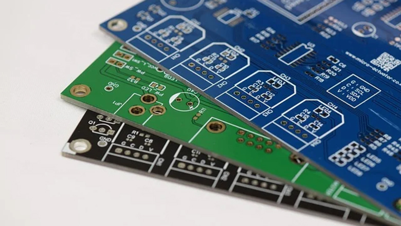
Physical Aspects and Board Substrates
- Size of Board:Dictated by the enclosure or application; a modern printed circuit board may range from millimeters for wearables to feet for telecom base stations.
- Board Substrate:The backbone material (FR4, polyimide, ceramic) directly impacts the mechanical and thermal performance of the physical circuit board.
- Board Shape:Custom shapes are often designed for modern products, optimizing use of enclosure space and enabling creative, ergonomic designs.
- Sides of the Board:Single and double-sided PCBs allow for different component densities. Multi-layer designs support more complex circuits and advanced PCB design strategies.
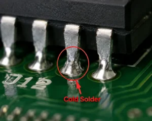
Assembly Process: Soldering and Mounting
After fabrication, the next step is printed circuit board assembly (PCBA).
Methods Used in PCB Assembly
Surface Mount Technology (SMT):
Electronic components are mounted on the surface of the Printed Circuit Board (PCB). The soldering process of these components is typically completed in a reflow oven.
This type of printed circuit board is suitable for advanced design and high-density circuits. It is commonly applied in the manufacturing of circuit boards for smartphones, computers and other modern electronic devices.
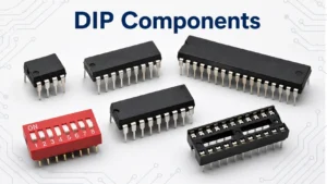
Through-Hole Construction:
Leads of electronic components are inserted into plated holes and soldered to the board.
Useful for components that require greater mechanical stability or must handle higher current.
Mixed Assembly:
This assembly process integrates Surface Mount Technology (SMT) and Through-Hole Technology (THT), and is mainly applied to the automotive and aerospace fields. The circuit boards required in these fields are typically large in size and impose extremely high requirements on reliability.
Key Assembly Steps:
- Solder paste application
- Pick-and-place (automated or manual placement of components on the board)
- Reflow or wave soldering
- Manual soldering (for specialized or low-volume boards)
- Inspection and testing
Expert Insight: Engineers must take full account of the specific sizes of solder pads, reasonable clearances of solder masks and the accuracy of placement data in the design process to ensure that solder joints achieve the highest level of reliability. The presence of such design defects often leads to performance malfunctions and results in high rework costs.
PCB Testing and Quality Control
PCB testing is a critical step to ensure the reliability of the overall design. Modern printed circuit boards are advancing toward higher density and greater complexity. This trend makes comprehensive and effective testing particularly important.
Common Testing Methods
- Automated Optical Inspection (AOI):Detects placement, polarity and soldering issues at high speed.
- In-Circuit Testing (ICT):Probes each node of the circuit for electrical values and correct function.
- Functional Testing:Simulates the operating environment, checking that the entire board and all board assemblies perform as specified.
- Flying Probe Testing:Ideal for prototypes and new PCB designs, requiring no expensive test fixtures.
Quality Control Factors
- Design for Test (DFT):Involved in PCB design from the beginning, DFT ensures test points and diagnostic features are easily accessible.
- Certification and Compliance:Rigid PCB manufacturing for critical applications requires ISO, IPC class, and/or RoHS compliance—especially in industrial electronics and aerospace.
Advanced PCB Design Techniques

The leap from board design basics to advanced PCB design unlocks innovation in the electronics industry. Here’s how cutting-edge designers and PCB manufacturers push boundaries:
Strategies for Advanced Design
- High-Density Interconnect (HDI):Uses microvias, fine-pitch components and thin copper layers to shrink the circuit even further for smartphones and tablets.
- 3D Printed PCBs:Allow for unique board shapes and direct integration into product enclosures, serving prototyping and custom device needs.
- Rigid-Flex and Stretchable PCBs:Used for advanced wearables, aerospace and medical devices to fit unconventional spaces and endure mechanical stress.
- Controlled Impedance Routing:Vital for digital design and radio-frequency circuits, where signal integrity is more critical than ever.
- Thermal Management:Integrating metal-core substrates, thermal vias and heat sinks extends the lifespan of high-power board assemblies.
Challenges in Board Design & Industry Trends
Common Challenges
- Miniaturization:High circuit density on a small board means strict design considerations for heat management, trace routing and manufacturability.
- Supply Chain Volatility:Sourcing advanced materials used in PCBs and certain ICs can delay projects—always design with available substitutes in mind.
- Green Manufacturing:Environmental regulations push the adoption of eco-friendly board substrates and lead-free processes.
- Design Collaboration:As teams become global, managing design data/version control and clear documentation is crucial.
The Future of the PCB Industry
- Printed circuit board manufacturing is embracing automation, AI-driven layout and real-time analytics for process optimization.
- 3D modeling and simulation are now core to the PCB design process, improving both speed and accuracy.
- Mass customization is enabled by 3D printed and rapidly fabricated boards.
- Global PCB manufacturers are investing in sustainable processes and recyclable materials, responding to pressure from tech giants and regulators.
- Integration of electronics and mechanics (mechatronics) is resulting in more sophisticated physical circuit board designs directly interfacing with sensors, actuators and advanced ICs.
Frequently Asked Questions about PCBs
What are the most common types of PCBs?
Single-sided, double-sided, multi-layer, rigid, flex and rigid-flex PCBs. Each is chosen based on the requirements of the circuit and the physical space available.
How do I get started with the intro to PCB design?
Start by learning circuit schematics, practice with free PCB design tools (like KiCad), and study open-source board designs. Move on to designing prototypes, experimenting with materials used, and connecting with PCB manufacturers for feedback.
Why does the material used in a PCB matter so much?
Material affects everything: electrical performance (especially at high frequency), heat management, board rigidity, cost and regulatory compliance.
What is the difference between a PCB and an integrated circuit?
A PCB hosts and connects various electronic components, including one or many integrated circuits; an integrated circuit is a single piece of silicon containing electronic circuits.
What are rigid and flexible PCBs best suited for?
Rigid PCBs work well for most general electronics, while flexible PCBs enable high-durability and unique shape circuits in wearables, medical and aerospace.